category » Research Abstracts
InGaAs is a promising candidate for channel material for future high-performance CMOS logic applications because of its superior electron transport…
A variety of compact MOSFET models are used for circuit simulation in both industry and academia, ranging from standard industrial…
The need for high speed and density in modern integrated circuits requires new MOSFET channel materials, techniques for improved carrier…
Historically, digital logic devices are benchmarked by the on-state current (Ion) at specified off-state current (Ioff) and supply voltage (Vdd)…
Recently, the demonstration of spin injection and transport in hybrid organic semiconductor (OS)-based devices [1] [2] [3] and the…
Organic photovoltaics (OPVs) are promising low-cost solar cells: they can be stacked in multi-junctions, and they are compatible with roll-to-roll…
Singlet exciton fission may find application in more efficient solar cells. Fission can reduce thermalization losses because by splitting the…
Over the last decade, quantum information experiments with trapped ions have demonstrated essential steps towards quantum computing and quantum simulation…
Superconducting nanowire avalanche photodetectors (SNAPs) [1] are based on a parallel architecture that performs single-photon counting with higher signal-to-noise ratio…
In this study, we demonstrated a high-resolution method for doubling the spatial frequency of lines and dots of structures defined…
A commercially-available scanning-helium-ion microscope of high source brightness [1] has been modified for operation with neon gas. This neon system…
Paracrine and autocrine cell signaling are critical factors guiding tissue development and maintenance, and dysregulation of these cues contributes to…
The high-frequency variability characterization of MOSFETs is becoming more necessary due to new process developments such as high-K metal gates,…
Technology scaling has enabled low-power operations in digital integrated circuits. Therefore, the trend to move analog-to-digital operations upstream to allow…
In CMP process, the pad asperity modulus and asperity height are two important properties that affect the planarization results [1]…
In this work we propose a particle agglomeration model for CMP, to understand the creation and behavior of agglomerated slurry…
Electromechanical resonators such as quartz crystals, surface acoustic wave (SAW) resonators, and ceramic resonators have become essential components in electronic…
As continued scaling becomes increasingly difficult, 3D integration has emerged as a viable solution to achieve higher bandwidth and power…
We seek to fabricate massively parallel waveguide lithium niobate spatial light modulators as an enabling technology for the next generation…
The efficient absorption and emission of light is of fundamental importance to the operation of optoelectronic devices such as solid-state…
The strongly coupled states of light and matter in microcavities known as polaritons offer exciting possibilities for the study of…
Photovoltaic cells containing nanoscale phase separated mixtures of a poly(thiophene) donor and a fullerene acceptor in the active layer have…
Solar cells based on lead sulfide colloidal quantum dots (PbS QDs) have demonstrated recent improvements in both efficiency and stability…
There is emerging interest in the ability to produce low-cost and lightweight solar cells and other electronics on flexible, stretchable,…
The low energy density of solar illumination necessitates deployment of solar technologies over large surface areas in order to capture…
It is desirable to extend the functionality of MEMS to different form factors including large area arrays of sensors and…
In recent years, there has been an increasing interest in the use of PbS and PbSe quantum dots (QDs) for…
It has been known for several decades that polymers doped with conducting particles, for example silicone nickel nano-particles, will exhibit…
As demands for high storage density, high chip memory capacity, and decreasing process costs continue to mount, conventional flash memory…
Colloidal quantum dots (QDs) are semiconductor nanoparticles that can be used in monolayers in low operating-voltage, non-lithographically fabricated, thin film…
J-aggregates, which are self-assembling molecular nanostructures [1] , have unique optical properties resulting from coherent coupling of their molecular components….
Colloidal quantum-dot light-emitting diodes (QD-LEDs) combine the thin film processability of organic materials with the tunable optical properties conferred by…
The non-destructive chemical mapping of surfaces with single-molecule sensitivity and sub-5-nm lateral resolution is an extraordinary challenge. Optical techniques such…
Transformation of solar energy into chemical fuels is an attractive energy conversion transformation to address the intermittency of power generation…
An ultrasound image is formed from a collection of ultrasonic beams transmitted and received by an array of transducer elements. …
Malaria prevails mainly in the countries that lack proper medical facilities, and it kills about a million people worldwide a…
Microsensor networks have applications ranging from environmental and industrial monitoring to wearable and implantable medical devices. Despite the breadth of…
Low-power portable electronics such as implantable medical devices require low-access-energy non-volatile memory to deliver longer battery lifetime and richer functionality….
On-chip memories are responsible for a large portion (40% by many estimates) of the total energy consumption and area of…
The use of video is becoming an important part of today’s world, and consumers are constantly demanding high-definition performance. In…
Circuits for wearable vital sign monitors have very stringent requirements on power dissipation due to limited energy storage capacity. Extending…
During recent years, researchers of the Electronic Design Automation community have made a great effort to develop new techniques for…
Standard boundary element methods (BEMs) involve both an embarrassingly parallelizable system setup step and a linear system solving step of…
Understanding certain medical conditions requires understanding specific aspects of the blood flow in the arterial network. For instance, diagnosing atherosclerosis…
Thin Film Bulk Acoustic Resonators (FBARs) are widely used in the design of modern radio frequency components including duplexers, filters,…
Parameterized model order reduction (PMOR) techniques can generate compact models reflecting the impact induced by design or process variations [1]…
Standard full chip capacitance extraction algorithms rely for computational efficiency on 2D scanning and table lookup algorithms. These algorithms trade…
Two recent advances in Magnetic Resonance Imaging (MRI) technology have resulted in a need for sophisticated computational electromagnetics (CEM) tools….
With modern digital communications applications moving towards increasingly high data rates, efficient spectral use requires modulation with dense constellations. The…
This project aims to develop a device to monitor tremor for treatment of neurological disorders such as Parkinson’s disease (PD)….
The proposed research program has two primary goals. The first goal is to improve the evaluation and treatment of patients…
With the continued communication systems trend towards high data rates come increasingly high signal bandwidths. If the carrier frequency is…
The scaling of MOSFETs in recent years has pushed the gate length down to less than 20 nanometers. Further gate…
The GaN high-electron-mobility transistor (HEMT) is a very promising device for power-switching applications due to the outstanding material properties of…
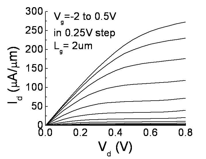
As conventional Si CMOS scaling approaches the end of the roadmap, III-V based field-effect transistors appear as an increasingly viable…
In Si p-type metal-oxide-semiconductor field-effect transistors (MOSFETs), the incorporation of mechanical strain in the channel has greatly enhanced hole velocity…
Achieving a sharp subthreshold swing is crucial to enable the supply voltage scaling that is necessary for reducing power consumption…
DNA damage has been found to play critical roles in cancer, aging, and heritable disease. There is rising interest in…
Front-end integration of III-V compound semiconductor devices with Si metal-oxide-semiconductor (MOS) technology requires the development of commercially viable engineered substrates…
We are developing materials for thermoelectric and thermophotovoltaics applications. Our objective is to develop III-V and/or IV superlattices with low…
Monolithic integration of III-V devices with Si CMOS technology allows us to combine the unique capabilities of III-V devices with…
Photovoltaics and sustainability have received a lot of attention lately. We seek a tandem photovoltaic device using silicon as both…
This paper discusses a way to optimize the In0.53Ga0.47As quantum-well MOSFET structures from the prospective of channel mobility. We experimentally…
Protective coatings that prevent the ingress of water into electronic devices fabricated on flexible plastic substrates are essential to extend…
The development of biosensors is considered a focal subject for clinical applications. The main efforts are being addressed towards in-vivo…
Aptamers are emerging as popular alternatives to antibodies as affinity probes in immunoassays. From a point-of-care diagnostics standpoint, aptamers have…
The mechanical properties of tissues and cells have important implications on their differentiated state, functions and responses to injury. Altered…
We present an integrated microfluidic probe that captures the contents of selected single adherent cells from standard tissue culture platforms…
Uniaxial strained Ge “nanobars” are of interest for future sub-10-nm gate length p-MOSFETs because of the excellent electrostatic control afforded…
Germanium is a promising candidate for use in CMOS-compatible photodiodes. Its strong absorption in the 1.55-µm range and relative ease…
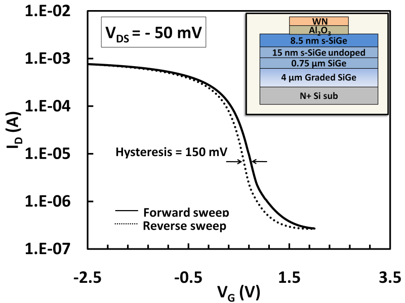
The type-II band alignment between strained-silicon (s-Si) and strained-germanium (s-Ge) has been proposed for use in tunneling transistors due to…
The terahertz frequency range (1-10 THz) has long remained undeveloped, mainly due to the lack of compact, coherent radiation sources….
Tumor invasion has received considerable attention as a critical step in cancer metastasis, and is a promising target for developing…
We recently demonstrated a process of thermal ink jet printing of PZT thin films for MEMS applications [1] [2] . …
In this project, a piezoelectric 2-D array of ultrasound transducers will be developed for compact, portable 3-D ultrasound imaging systems….
To overcome the limitations of piezoelectric energy harvesters such as narrow bandwidth and low power density, our group has recently…
Hexagonal boron nitride (hBN) is very attractive for a variety of applications, particularly as deep ultraviolet emitter, transparent membrane, dielectric…
As process technology scales, the importance of material and architectural innovation for interconnect performance will continue to increase. Graphene has…
Organic photovoltaics (OPV) has gained much attention as a possible candidate for the next generation of clean electricity due to…
Passive components, namely inductors, transformers, and capacitors, are often the largest and most expensive components in power electronic circuits, and…
A novel sensing technology for unmanned undersea vehicles (UUVs) is under development. The project is inspired by the lateral line…
In zero-crossing based circuits (ZCBC), op-amps in pipelined ADCs are replaced with zero-crossing detectors (ZCDs). The closed-loop feedback provided by…
There is an ever-increasing demand for high resolution and high accuracy in A/D converters in communication systems. In order to…
Most current ultrasound imaging systems use piezoelectric materials for the ultrasound transducer. The recent development of micro-electromechanical systems (MEMS) allowed…
Technology scaling poses challenges in designing analog circuits because of the decrease in intrinsic gain and reduced swing. An alternative…
Energy efficiency and power savings are of paramount importance in the ever-increasing use of implantable and portable medical devices. Front-end…
Wireless communication technology is rapidly advancing, and new wireless applications are continuously developed. Figure 1 shows each application and the…
Electric Propulsion (EP) brings benefits for space missions requiring relatively large changes in satellite velocity, for example by reducing the…
Using suspended nanochannel resonators (SNRs), we demonstrate measurements of mass in solution with a resolution of 27 ag in a…
Precision frequency detection has enabled the suspended microchannel resonator (SMR) to weigh single living cells, single nanoparticles, and adsorbed protein…
Under the pressure of increasing population, crowded traffic, the energy crisis, and environmental concerns, current transportation systems have run into…
The formation of organic molecular nano-crystals is a topic of great interest in the pharmaceutical industry because of the potential…
The high-frequency performance of Ga-face AlxGa1–xN/GaN high electron mobility transistors (HEMTs) has rapidly increased in recent years, enabling use of…
Gallium nitride (GaN) is a wide bandgap semiconductor with unsurpassed properties for high voltage switches and RF amplifiers. However, in…
AlGaN/GaN high electron mobility transistors (HEMTs) have attracted a great interest for the next generation of power electronics due to…
Thanks to its all-surface 2D structure combined with a very high carrier mobility, graphene is a very promising candidate for…
GaN-based transistors have outstanding properties for the development of ultra-high efficiency and compact power electronics. The high electron mobility in…
The use of gate dielectrics in AlGaN/GaN high electron mobility transistors (MIS-HEMTs) is attracting great interest for power applications since…
The combination of high critical electric field, carrier mobility and thermal stability makes GaN an ideal semiconductor for power switches…
Graphene is a one-atom-thick layer of carbon atoms arranged in a honeycomb lattice through sp2 bonding [1] . Considered for…
Graphene is a two-dimensional (2D) material that has attracted great interest for electronic devices since the demonstration of field effect…
Designing on-chip networks optimized for a cache coherence protocol is critical for many-core processors to achieve peak efficiency in energy,…
Recent technological advances in three-dimensional (3D) semiconductor fabrication have provided an implementation platform for powerful multicore, multiprocessor, and network-on-chip (NoC)…
With nearly 1.6 billion people living without electricity, the demand for small-scale distributed power generation is high. In developing countries,…
Mammalian cell cultures dominate the biopharmaceutical industry because their products, valuable biotherapeutics including monoclonal antibodies, vaccines and growth factors, account…
For systems biology, the models are more often limited by the absence of reliable experimental data than by available computational…
Carbon nanotubes (CNTs) are excellent heat spreaders for packaging electronic/photonic devices due to their high thermal conductivity and good mechanical…
We are investigating the performance of low-noise, high-power optoelectronic oscillators (OEO) using all slab-coupled optical waveguide (SCOW) components. The optoelectronic…
Nonlinear optics comprises a rich body of physics that could enable a number of interesting functionalities in integrated silicon photonics…
Low propagation loss deposited waveguides are an important component to enable photonic integration in the majority of high-volume electronics processes….
We are investigating thermoelectric transport in light-emitting diodes (LEDs). Electro-luminescent cooling is a phenomenon in which the optical output power…
There exists great interest in the utilization of the human body as a possible power supply for running such electronics…
Surface plasmon polaritons (SPPs) are optical waves that propagate at the interface between a metal and a dielectric, and can…
We are studying BiFeO3/CoFe2O4 oxide composite thin films, which have the remarkable characteristic of self-assembling into vertical nanostructures during their…
We have experimentally demonstrated a monolithically integrated ultra-compact optical isolator on silicon. This device uses a different design strategy from…
We are interested in using ferromagnetic materials to engineer more energy-efficient transistors and logic gates. Transistors today are limited by…
Self-organized macromolecular materials can provide an alternative pathway to conventional lithography for the fabrication of devices on the nanometer scale….
Block copolymer self-assembly on nanolithographically-defined templates has great potential in fabricating patterned media and devices at the nanometer scale. Current…
We maintain a thin-film laboratory that includes a pulsed-laser deposition (PLD) system and an ultra-high vacuum sputter system. The PLD…
The success of nanoparticles (NPs)-based devices requires reliable fabrication methods for well-defined, defect-free self-assembled NP structures. NP self-assembly is a…
Many domain wall (DW) devices require the presence of multiple DWs, each of which may need to be independently controlled…
We are investigating the fabrication and magnetic properties of rings (Figure 1) for magnetic logic and memory devices. The magnetic…
Magnetic metal nanoparticle arrays have attracted considerable interest for applications in patterned magnetic recording media as well as catalyst arrays…
Block copolymers can be used to make a variety of functional electronic or magnetic devices. We have developed pattern transfer…
Triblock terpolymers are interesting because they can form a much wider diversity of 3D structures than diblock copolymers, including rings…
We have designed an ultra-low-power 32-channel neural recording system in a 0.18-µm CMOS technology. The system consists of eight neural…
To achieve comfortable form factors for wireless medical devices, battery size, and thus power consumption, must be curtailed. Often the…
The Capacitive Micromachined Ultrasound Transducer (CMUT) is an alternative to traditional piezoelectric transducers. The CMUT technology provides an opportunity for…
Epilepsy is a common chronic neurological disorder that affects about 1% of the world population [1] . It is characterized…
Vital signs such as heart rate, blood pressure, blood oxygenation, cardiac output, and respiratory rate are necessary in determining the…
Intracranial pressure (ICP) is a key factor in monitoring a patient’s cerebrovascular state. However, current ICP measurement modalities are highly…
With the escalating costs of hospital visits, clinicians are opting to use at-home monitoring devices to diagnose patients. Current ECG…
Implantable medical sensors are an emerging application area that exemplifies the stringent energy constraints imposed on wireless sensor circuits. In…
Power gating has become ubiquitous in ICs to reduce the power consumed by inactive CMOS logic circuits. However, the finite…
In today’s large systems-on-a-chip, communication infrastructure such as high-speed I/Os consumes a significant portion of power, limiting the amount left…
Material properties are defined not only by the composition, but by structure as well. Such materials are suited for use…
Vapor deposited thin films are rarely stable, so that when they are heated to temperatures at which atomic diffusivities are…
Improvements in electrochemical devices for energy storage (Li-based batteries and ultracapacitors), and capacitive deionization are being aggressively investigated. There are…
Polycrystalline metallic thin films are vital in a wide variety of applications, including microelectronics, plasmonics, magnetic storage, N/MEMS and catalysis. …
Capacitors have attracted considerable attention due to their potential as an energy buffer in a hybrid energy system. Improvement of…
Combustion of fossil fuels, essential for electricity generation and vehicular propulsion, is generally incomplete, leading to harmful NOx, CO, and…
Solid oxide fuel cells (SOFCs) directly convert chemical to electrical energy with high efficiency and can operate using a wide…
Detection of high-energy radiation (e.g., γ-rays) is key in nuclear non-proliferation strategies. When a wide-band gap semiconductor detector intercepts a…
With continuously growing energy demands, new alternative energy solutions become essential. In order to achieve sustainability, efficient conversion and storage…
Gas sensors are essential in the monitoring, control, and reduction of harmful emissions in the environment [1] . Conductometric gas…
One of the most fundamental technical problems concerning spacecraft design is preparing the vehicle to survive the extreme conditions encountered…
Field Emitter Arrays (FEAs) are excellent cold cathodes, but they have not found widespread adoption in demanding device applications because…
Retarding potential analyzers (RPAs) were first developed in the 1960’s. RPAs find widespread application including characterization of near-spacecraft environments and…
This project aims to develop the technology for field-enabled low-power portable vacuum sources that can be made cheaply and reliably,…
There is a need for microscale vacuum pumps that can be readily integrated with other MEMS and electronic components at…
Organic semiconductor-based devices can easily be scaled to large areas and fabricated on flexible, elastic, and non-planar surfaces at low…
A near-ultraviolet (UV) sensor based on zinc oxide (ZnO) nanowires (NWs) that is sensitive to photo excitation at or below…
An electrospray emitter ionizes polar liquids using high electrostatic fields. The electric field produces suction on the free surface (meniscus)…
Optically transparent, wide band gap metal oxide semiconductors are a promising candidate for large area flexible electronics. Because most commercially…
Many immune responses are mediated by cell-cell interactions. In particular, cytotoxic T cells form conjugates with pathogenic and cancer cells…
The use of microsystems to manipulate and study cells in microenvironments is continually increasing. However, along with such increase in…
Stem cell phenotype and function are influenced by microenvironmental cues that include cell-cell, cell-extracellular matrix (ECM), and cell-media interactions, as…
Autocrine signaling is a mode of chemical signaling that occurs when cells can capture self-secreted diffusive factors. Apart from its…
The development of new techniques to separate and characterize cells with high throughput has been essential to many of the…
Microfabricated/microfluidic approaches to cell sorting, include purely dielectrophoretic (DEP) trap arrays [1] , passive hydrodynamic trap arrays with active DEP-based…
Significant interest exists in creating insect-based Micro-Air-Vehicles (MAVs) [1] [2] [3] that would combine advantageous features of insects—small size, effective…
The mechanism of critical heat flux (CHF) is commonly attributed to two limits during boiling behavior: 1) the hydrodynamic limit…
The most common substrate for processing chemical vapor deposition (CVD) graphene and highly oriented pyrolytic graphite (HOPG) has been thermally…
Superconducting nanowire single-photon detectors (SNSPDs) [1] perform single-photon counting in the near‑infrared with outstanding performance. The main limitations of standard…
Luneburg lens is a gradient index (GRIN) element [1] known to produce diffraction-limited focus at the lens edge opposite to…
Templated self-assembly of block copolymer, based on topographic templates defined by electron-beam lithography (EBL), is an attractive candidate for next…
Semiconductor quantum dots (QDs) are electronically-quantized systems with promising applications in optoelectronic devices [1] . A key aspect of such…
Compact models describing the voltage-dependent terminal current and charges (or equivalently, capacitances) are essential for small-signal and transient circuit simulation. …
Exciton transport is universal in every kind of organic optoelectronic devices – including organic light-emitting diodes (OLEDs) and organic solar…
Photolithography’s accuracy and scalability have made it the method for sub-micron-scale definition of single-crystal semiconductor devices for over half a…
Luminescent Solar Concentrators (LSCs) aim to reduce the cost of solar electricity by using an inexpensive collector to concentrate solar…
Many on-chip optical applications, including spectroscopy [1] ; sensing [2] [3] ; nonlinear optics [4] [5] [6] ; and optical…
Organic photovoltaics (OPVs) are promising low-cost solar cells: they can be stacked in multi-junctions, and they are compatible with roll-to-roll…
Photovoltaic solar concentrators aim to increase the electrical power obtained from solar cells. Conventional solar concentrators track the sun to…
In recent years there has been significant interest in broadband, omnidirectional antireflection (AR) nanostructures that minimize Fresnel reflection due to…
Selective detection of explosive compounds is critical for national defense and homeland security. Nitroaromatic compounds pose a particular threat; 2,4,6-trinitrotoluene…
Our ongoing research integrating 1.55-µm III-V ridge waveguide gain elements (i.e., diode lasers and semiconductor optical amplifiers) co-axially aligned with…
Optogenetics is commonly used for precision modulation of the activity of specific neurons within neural circuits [1] , but assessing…
The use of magnetic forces to improve fluidic self-assembly of micro-components has been investigated using Maxwell 3D to model the…
Optoelectronic devices intimately integrated on silicon integrated circuits have long been sought for optical intercon-nect applications, optical communications modules, and–more…
Professor Ed Boyden uses light to precisely control neural activity. His lab has invented safe, effective ways to deliver light-gated…
GaN-based high electron mobility transistors (HEMTs) have great potential for high power/frequency applications due to their outstanding combination of large…
Carbon nanotube (CNT) composites are promising new materials for structural applications thanks to their mechanical and multifunctional properties. We have…
We integrated ultra-porous (99% porous) elements composed of nanoporous forests of vertically aligned carbon nanotubes (VACNTs) in MEMS, demonstrating their…
Characterization of thin film layered materials is critical for many MEMS devices. Residual stresses from production determine both final shape…
The recent development of “low power” (10s-100s of μW) sensing and data transmission devices, as well as protocols with which…
Vertically-aligned carbon nanotube (CNT) arrays are grown on a moving substrate, demonstrating continuous growth of nanoscale materials with long-range order….
Catastrophic structural failures are the cause of many physical and personal losses, with prevention estimated at billions of dollars in…
This work focuses on development of non-metallic substances that can catalyze carbon nanotube (CNT) growth while remaining in a non-metallic…
Two of the greatest challenges in MEMS are those of packaging and integration with CMOS technology. Development of unreleased MEMS…