Fabrication of GaAs-on-Insulator via Low-temperature Wafer Bonding and Sacrificial Etching of Ge by XeF2
- Category: Materials
- Tags: Eugene Fitzgerald, Yu Bai
Front-end integration of III-V compound semiconductor devices with Si metal-oxide-semiconductor (MOS) technology requires the development of commercially viable engineered substrates [1] [2] . The fabrication of engineered substrates currently utilizes technologies such as epitaxy, wafer bonding, and layer exfoliation. We report on the development of GaAs-on-insulator (GaAsOI) structures without the use of SmartcutTM technology. GaAs/Ge/GaAs epitaxial stacks containing an embedded Ge sacrificial release layer were grown with metal-organic chemical vapor deposition (MOCVD) and exhibit both a low defect density as well as surface properties suitable for wafer bonding [3] . A room-temperature oxide-oxide bonding process was developed to enable the integration of substrates with a large difference in their coefficients of thermal expansion. The release of the donor substrate and transfer of the GaAs layer onto the handle substrate were realized through room-temperature, gas-phase lateral etching of an embedded Ge sacrificial layer by xenon difluoride (XeF2). Figure 1 schematically shows our fabrication process. This GaAsOI fabrication process is shown to be successful on a small scale. Figure 2 shows a cross-sectional TEM image of the final GaAsOI/Si structure fabricated with this process. Implementation of this process for fabricating large-area GaAsOI substrates is currently limited by the long diffusion distances required in a wafer-scale lateral etching process. We established a model that identifies the rate-limiting processes and potential approaches that lift these constraints and enable this method to be used for fabrication of large-diameter GaAsOI substrates.
-
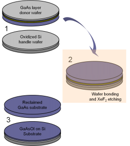
- Figure 1: GaAsOI fabrication process in this work: 1) Preparation of the bonding substrates: thermally oxidized Si handle wafer and GaAs donor wafer with GaAs/Ge/GaAs epitaxial stack covered with PECVD oxide. Si: dark grey, SiO2: light grey, GaAs: blue, Ge: dark yellow. 2) Low-temperature wafer bonding and room temperature spontaneous etching with XeF2 gas-removing sacrificial Ge layer. 3) After separation, GaAsOI on Si substrate and reclaimed GaAs donor substrate.

-
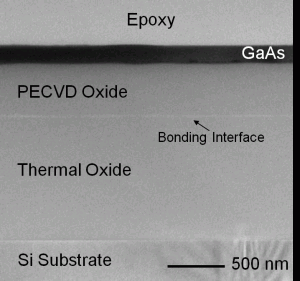
- Figure 2: XTEM image showing GaAsOI/Si structure with high quality bond interface obtained with our low-temperature fabrication process.

- C. L. Dohrman, K. Chilukuri, D. M. Isaacson, M. L. Lee, and E. A. Fitzgerald, “Fabrication of silicon on lattice-engineered substrate (SOLES) as a platform for monolithic integration of CMOS and optoelectronic devices,” Materials Science and Engineering B-Solid State Materials for Advanced Technology, vol. 135, pp. 235-237, Dec 15 2006. [↩]
- W. K. Liu, D. Lubyshev, J. M. Fastenau, Y. Wu, M. T. Bulsara, E. A. Fitzgerald, M. Urteaga, W. Ha, J. Bergman, B. Brar, W. E. Hoke, J. R. LaRoche, K. J. Herrick, T. E. Kazior, D. Clark, D. Smith, R. F. Thompson, C. Drazek, and N. Daval, “Monolithic integration of InP-based transistors on Si substrates using MBE,” Journal of Crystal Growth, vol. 311, pp. 1979-1983, Mar 15 2009. [↩]
- Y. Bai and E. A. Fitzgerald, “Ge/III-V heterostructures and their applications in fabricating engineered substrates,” Electrochemical Society Transactions, vol. 33, pp. 927-932, 2010. [↩]