Compact Physical Modeling of Graphene Field Effect Transistors
- Category: Electronic Devices
- Tags: Dimitri Antoniadis, Han Wang, Jing Kong, Tomas Palacios
Graphene is a two-dimensional (2D) material that has attracted great interest for electronic devices since the demonstration of field effect carrier modulation in 2004 [1] . Its high mobility and high saturation velocity make graphene a promising material for next generation of high-frequency devices [2] , and its 2D geometry also makes it highly compatible with existing fabrication technology in the semiconductor industry. Furthermore, the possibility of large-scale synthesis of graphene by chemical vapor deposition (CVD) and epitaxial growth [3] [4] [5] makes graphene integrated circuits a feasible reality in the near future. Hence, it is desirable to develop a compact physical model that can enable the use of computer-aided-design software to simulate future complex circuits. In this work, we develop a compact model for the current-voltage characteristics of graphene field effect transistors (GFETs), which is based on an extension of the “virtual-source” model previously proposed for Si MOSFETs [6] [7] and is valid for both saturation and non-saturation regions of device operation (Figure 1). This virtual source model provides a simple and intuitive understanding of carrier transport in GFETs, allowing extraction of the virtual source injection velocity vVS, a physical parameter with great technological significance for short-channel graphene transistors. With only a small set of fitting parameters, the model shows excellent agreement with experimental data (Figure 2). It is also shown that the extracted virtual source carrier injection velocity for graphene devices is much higher than in Si MOSFETs and state-of-the-art III-V HFETs with similar gate length, supporting the great potential of GFETs for high frequency applications. Future work includes extending the model for both small signal and large signal modeling of GFETs RF performance and implementation in Verilog to enable modeling of graphene circuits.
-
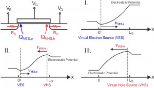
- Figure 1: Schematic diagram of the cross-section of a GFET device. The virtual electron source (VES) point and the virtual hole source (VHS) point in the channel are defined for a GFET. The electrostatic potential along the channel and the position of VES and VHS are shown for a GFET operating in the three operating regions: I. Electron conduction region; II. Ambipolar region; III. Hole conduction region.

-
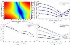
- Figure 2: (a) Top-view of the three-dimensional plot of IDS vs. VTGS and VBGS at VDS=1.1 V. (b), (c) and (d) are cross-sections in (a) at the corresponding dotted lines. The model results are shown as solid lines; the experiment data is shown as dots. In (b), VBGS is kept constant at 0 V, and VTGS is swept from -1 V to 3 V. A family of curves is shown for VDS increasing from 0.35 V to 1.1 V in steps of 0.25 V. In (c), VTGS is kept constant at 0 V, and VBGS is swept from -50 V to 100 V. (d) VTGS is kept constant at 1.41 V, and VBGS is swept from -30 V to 40 V. A family of curves is shown for VDS, increasing from 0.35 V to 1.1 V in steps of 0.25 V.

- K. S. Novoselov, et al., “Electric field effect in atomically thin carbon films,” Science, vol. 306, pp. 666-669, Oct. 2004. [↩]
- T. Palacios, et al. “Applications of graphene devices in RF communications,” IEEE Comm. Mag., vol. 48, no. 6, pp. 122-128, June 2010. [↩]
- A. Reina, et al., “Large area few-layer graphene films on arbitrary substrates by Chemical Vapor Deposition,” Nano Lett., vol. 9, no. 1, pp. 30-35, Jan. 2009. [↩]
- X. Li, et al. “Large-area synthesis of high-quality and uniform graphene films on copper foils,” Science, vol. 324. no. 5932, June 2009. [↩]
- C. Berger, et al. “Electronic confinement and coherence in patterned epitaxial graphene,” Science, vol. 312. no. 5777, May 2006. [↩]
- A. Khakifirooz, O. M. Nayfeh, and D. Antoniadis “A simple semiempirical short-channel MOSFET current-voltage model dontinuous across all regions of operation and employing only physical parameters,” IEEE Trans. Electron Devices, vol. 56, no. 8, Aug. 2009. [↩]
- D. A. Antoniadis, I. Åberg, C. N. Chleirigh, O. M. Nayfeh, A. Khakifirooz, and J. L. Hoyt, “Continuous MOSFET performance increase with device scaling: The role of strain and channel material innovation,” IBM J. Res. Develop., vol. 50, no. 4/5, pp. 363–376, July 2006. [↩]