Platform for Monolithic Integration of III-V Devices with Si CMOS
- Category: Materials
- Tags: Eugene Fitzgerald, Nan Pacella
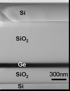
Monolithic integration of III-V devices with Si CMOS technology allows us to combine the unique capabilities of III-V devices with the economies of scale and established infrastructure of Si CMOS to create advanced circuits with new functionalities. We have developed the silicon-on-lattice-engineered-silicon (SOLES) substrate platform in order at accomplish this goal [1] [2] [3] [4] . The SOLES structure is a silicon substrate with an embedded III-V template. One version of it is illustrated in Figure 1. First, Si CMOS devices are fabricated on the top silicon-on-insulator layer due to their high thermal budget requirements. Once the Si devices are in place, the III-V template can be accessed by etching windows in the top Si and oxide. III-V device structures can then be grown from the III-V template to be coplanar with the CMOS devices. If these III-V devices are encapsulated with Si, CMOS silicide contacts can be made to both the Si and III-V in parallel.
InP metamorphic heterojunction bipolar transistors (mHBTs) and Si CMOS devices have been successfully integrated on SOLES wafers, although with traditional III-V and CMOS contact technology [5] . We are now working to establish a CMOS metallization scheme for III-V devices based on silicide technology. We are also developing improved versions of the SOLES structure, with direct incorporation of high quality III-V template layers.
- C. L. Dohrman, K. Chilukuri, D. M. Isaacson, M. L. Lee, and E. A. Fitzgerald, “Fabrication of silicon on lattice-engineered substrate (SOLES) as a platform for monolithic integration of CMOS and optoelectronic devices,” Materials Science and Engineering B: Solid-State Materials for Advanced Technology, vol. 135, no. 3, pp. 235-237, Dec. 2006. [↩]
- F. Letertre, “Formation of III-V semiconductor engineered substrates using Smart CutTM layer transfer technology,” in Mater. Res. Soc. Symp. Proc. 2008, vol. 1068, pp. 1068-C01-01. [↩]
- K. Chilukuri, M. J. Mori, C. L. Dohrman, and E. A. Fitzgerald, “Monolithic CMOS-compatible AlGaInP visible LED arrays on silicon on lattice-engineered substrates (SOLES),” Semiconductor Science and Technology, vol. 22, pp. 29-34, 2007. [↩]
- N. Yang, M. T. Bulsara, E. A. Fitzgerald, W. K. Liu, D. Lubyshev, J.M. Fastenau, Y. Wu, M. Urteaga, W. Ha, J. Bergman, B. Brar, C. Drazek, N. Daval, L. Benaissa, E. Augendree W. E. Hoke, J. R. LaRoche, K. J. Herrick, and T. E. Kazior, “Thermal considerations for advanced SOI substrates designed for III-V/Si heterointegration,” in 2009 IEEE International SOI Conference, pp. 121-122. [↩]
- W. K. Liu, D. Lubyshev, J. M. Fastenau, Y. Wu, M. T. Bulsara, E. A. Fitzgerald, M. Urteaga, W. Ha, J. Bergman, B. Brar, W. E. Hoke, J. R. LaRoche, K. J. Herrick, T. E. Kazior, D. Clark, D. Smith, R. F. Thompson, C. Drazek, and N. Daval, “Monolithic integration of InP-based transistors on Si substrates using MBE,” J. Crystal Growth, vol. 311, no. 7, pp. 1979–1983, Mar. 2009. [↩]
