Top-down Fabrication of N-face GaN/AlGaN Nanowire HEMTs
- Category: Nanotechnology
- Tags: Mohamed Azize, Tomas Palacios
The high-frequency performance of Ga-face AlxGa1–xN/GaN high electron mobility transistors (HEMTs) has rapidly increased in recent years, enabling use of these devices in power amplifiers for mm-wave applications [1] . However, this frequency performance is still far from the theoretical limit due to poor gate modulation efficiency, short channel effects and high access resistances. With their reversed polarization, N-face GaN/AlGaN transistors have a tremendous potential to improve device performance [2] . At the same time, nanowire (NW)-based HEMTs could also help to overcome many of these limitations and increase the maximum frequency of nitride devices by improving the electron confinement and reducing short channel effects [3] . Therefore, the combination of both N-face material and NW structures in the same device would offer new flexibility for high-frequency power amplifiers. We are developing NW-based nitride HEMTs to explore the maximum frequency performance of nitride devices [3] .
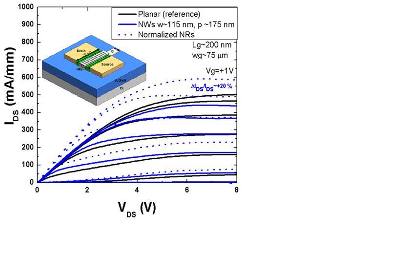
Our starting material is a Ga-face AlGaN (~17 nm)/GaN (~25 nm) /AlGaN (~5 nm)/GaN (~1.8 mm) HEMTs grown on Si(111) substrate by metal organic vapor phase epitaxy. After growth, the Ga-face of the wafer is bonded to a carrier substrate; dry etching removes the original substrate and GaN buffer to expose the N-face of the GaN/AlGaN structure (see Figure 1). With a 5-nm-thick etch stop layer, all GaN buffer can be removed, leaving only 47 nm of AlGaN/GaN/AlGaN structure. Free-standing NW devices are fabricated in a two-step, top-down technology [4] . Standard planar transistors are first fabricated; via electron-beam lithography, arrays of lateral NWs are patterned between two Ohmic contacts. Electron cyclotron resonance reactive ion etching removes the material between adjacent NWs by using BCl3 and Cl2 chemistry. The etch depth is ~ 50 nm, deep enough to prevent electrical conduction between NWs. A maximum drain current of ~600 mA/mm is measured in the fabricated NW-based HEMTs (see Figure 2). This current density is ~20% higher than current in a planar N-face HEMT, used as a reference. Characterization of the high frequency performance of these nanowires is currently underway. We expect that the large carrier confinement of these devices will allow higher operating frequencies as well as linearity. [5]
-
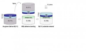
- Figure 1: Main processing steps of the layer transfer technology used to obtain N-face GaN epilayers.

-

- Figure 2: Ids-Vds characteristics of N-face planar and NW HEMTs. The current in NW devices is also normalized to the effective diameter (i.e., conducting channel) for a direct comparison between planar and NW-based HEMTs.
- J. W. Chung, W. E. Hoke, E. M. Chumbes, and T. Palacios, IEEE Electron Device Lett. vol. 31, p. 3, 2010. [↩]
- S. Rajan, A. Chini, M. H. Wong, J. S. Speck, and U. K. Mishra, J. Appl. Phys., vol. 102, p. 44501, 2007. [↩]
- B. Yu, Y. Yuan, J. Song and Y. Taur, IEEE Transactions on Electron Dev. vol. 56, p 2357, 2009. [↩] [↩]
- M. Azize and T. Palacios, App. Phys. Lett., vol. 98, p. 042103, 2011.2011. [↩]
- J. W. Chung, E. L. Piner, and T. Palacios, IEEE Electron Device Lett. vol. 30, p. 113, 2009. [↩]