Circuit for Characterizing TSV Stress-induced Variation
- Category: Circuits & Systems
- Tags: Duane Boning, Li Yu
As continued scaling becomes increasingly difficult, 3D integration has emerged as a viable solution to achieve higher bandwidth and power efficiency [1] . Through-silicon-via (TSV), which directly connects stacked structures die-to-die, is one of key techniques enabling 3D integration. The process steps and physical presence of TSVs, however, may generate stress-induced thermal mismatch between TSVs and silicon bulk. This effect could further perturb the performance of nearby electronic structures, particularly transistors, diodes, and associated circuits.
We propose a comprehensive study to characterize, analyze, and model stress impact on device and circuit performance induced by single and arrayed TSVs and its interaction with polysilicon and shallow-trench-isolation (STI) layout pattern density. A test chip is designed with multiplexing test circuits providing measurement of key parameters of large numbers of devices. These devices under test (DUTs) have layouts that explore a range of TSV and device layout choices in a layout experimental design (DOE). The test chip uses a scan chain approach combined with low-leakage and low-variation switches and Kelvin sensing connections, providing access to detailed analog device characteristics in large arrays of test devices.
The test structures are divided in three regions, as summarized below. (1) The 60×240 DUT transistor arrays are designed to characterize single TSV stress effects and their interactions with the pattern density and local layout pattern. In each region, a radius sampling scheme is proposed with different sampling distances and angles. Test structures are also designed with different Keep-Out-Zone materials and widths. (2) The 512×512 DUT transistor arrays are designed to characterize pattern density and multiple TSV stress effects. Long-range pattern density effects (STI, polysilicon and TSV pattern density) can also be tested in this region. (3) Four ring oscillators (ROs) with different RO spacing and TSV to transistor angle are designed to characterize single TSV stress effects on digital circuits. In each block, 128 groups of 17-stage ring oscillators with constant STI and poly density are designed to characterize TSV stress effects on circuit speed.
-
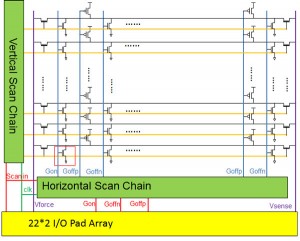
- Figure 1: Proposed multiple TSV and long-range pattern density induced variation characterization circuit approach for a mixed nMOS and pMOS transistor array.

-
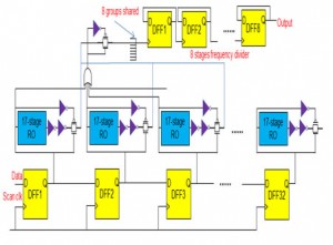
- Figure 2: RO test circuit block.

- S. Q. Gu et al. “Stackable memory of 3D chip integration for mobile applications.” IEEE International Electron Devices Meeting, vol. 33, no. 4, pp. 1-4, 2008. [↩]