High-speed Graphene Circuits and Photodetectors
- Category: Electronic Devices
- Tags: Allen Hsu, Jing Kong, Tomas Palacios
The most common substrate for processing chemical vapor deposition (CVD) graphene and highly oriented pyrolytic graphite (HOPG) has been thermally grown silicon dioxide on top of silicon. Due to optical interference, monolayer and bilayers of graphene can be easily identified using a standard optical microscope [1] . Furthermore, graphene is capacitively coupled to the underlying silicon, allowing for rapid electrical characterization through substrate biasing. While this substrate has proven useful for probing carrier transport in graphene as well as for developing graphene processing technology, the parasitic capacitances associated with the underlying silicon limit high-frequency performance. In this work, we have explored fabrication of graphene on purely insulating substrates, specifically sapphire. Sapphire is a common substrate used for radio frequency (RF) applications due to its low conductivity. Furthermore, it is much cheaper than other insulating substrates such as SiC or diamond.
Through recent advances in improved ohmic processing using an oxidized aluminum capping layer, we are able to fabricate high-speed field effect transistors on both silicon dioxide and sapphire [2] . Figure 1 shows measured RF data for a device with gate length (Lg) = 2 µm and width (W) = 25 µm on each substrate. While RF performance of graphene on silicon is slightly better after de-embedding than that of the sample on sapphire, we attribute this discrepancy to non-optimized processing conditions, possibly due to the transfer anneal or fabrication problems on transparent substrates. Fortunately, we are still able to achieve an extrinsic ft-Lg product of 14 GHz-µm on sapphire, which to our best knowledge is the highest reported extrinsic value on CVD graphene (Figure 2 [3] [4] [5] [6] [7] [8] ). In parallel, scanning photocurrent measurements of graphene on silicon dioxide show optical sensitivities of 0.4 mA/W for large-area devices (>375 µm2). Therefore, combining our results on sapphire with optical measurements should hopefully allow for large-area arrays of high-speed graphene photodetectors.
-
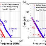
- Figure 1: RF performance between graphene on (a) 300-nm SiO2/Si and (b) sapphire. Values shown are extrinsic ft and de-embedded ft.

-
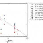
- Figure 2: Comparison of RF performance from devices from literature as well as silicon [3] [4] [5] [6] [7] [8] . Red symbols represent extrinsic performance (ft,ext); blue symbols are values after de-embedding (ft,deebmed). The dotted line is the performance of 90-nm SOI NMOS reported in [8] .

- X. Wang, M. Zhao, and D. D. Nolte, “Optical contrast and clarity of graphene on an arbitrary substrate,” Applied Physics Letters, vol. 95, p. 081102, 2009. [↩]
- A. Hsu, H. Wang, K. K. Kim, J. Kong, and T. Palacios, “Impact of graphene interface quality on contact resistance and RF device performance,” submitted for publication. [↩]
- J. S. Moon, D. Curtis, M. Hu, D. Wong, C. McGuire, P. M. Campbell, G. Jernigan, J. L. Tedesco, B. VanMil, R. Myers-Ward, C. Eddy, Jr., and D. K. Gaskill, “Epitaxial-graphene RF field-effect transistors on Si-face 6H-SiC substrates,” Electron Device Letters, vol. 30, pp. 650, 2009. [↩] [↩]
- Y. Wu, Y. Lin, A. A. Bol, K. A. Jenkins, F. Xia, D. B. Farmer, Y. Zhu, and P. Avouris, “High-frequency, scaled graphene transistors on diamond-like carbon,” Nature, vol. 472, p. 74, 2011. [↩] [↩]
- Y. Lin, C. Dimitrakopoulos, K.A. Jenkins, D. B. Farmer, H.Y. Chiu, A. Grill and P. Avouris, “100-GHz Transistors from wafer-scale epitaxial graphene,” Science vol. 327, p. 662, 2010. [↩] [↩]
- Y. Lin, K. A. Jenkins, A. Valdes-Garcia, J. P. Small, D. B. Farmer and P. Avouris, “Operation of graphene transistors at gigahertz frequencies,” Nano Lett., vol. 9, p. 422, 2009. [↩] [↩]
- L. Liao, Y. C. Lin, M. Bao, R. Cheng, J. Bai, Y. Liu, Y. Qu, K. L. Wang, Y. Huang, and X. Duan, “High-speed graphene transistors with a self-aligned nanowire gate,” Nature, vol. 467, p. 305, 2010. [↩] [↩]
- J. Plouchart, J. Kim, J. Gross, R. Trzcinski, and K. Wu, “Scalability of SOI CMOS technology and circuit to millimeter-wave performance,” presented at CSIC Symposium 2005. [↩] [↩] [↩]