Bias Stress Effect in PbS Quantum Dot Field Effect Transistors
- Category: Electronic Devices
- Tags: Tim Osedach, Vladimir Bulovic
In recent years, there has been an increasing interest in the use of PbS and PbSe quantum dots (QDs) for optoelectronic device applications. Much remains poorly understood about charge transport in thin films of these materials, however. In several recent studies of lead chalcogenide QDs in field effect transistor (FET) structures, a fast bias stress effect, or shift in threshold voltage (ΔVth) under prolonged gate bias, was observed [1] [2] [3] [4] . This effect manifests as a stretched-exponential decay in the drain-source current (Ids) and is usually attributed to screening of the gate field by the trapped charge. The instability associated with bias stress precludes many practical applications of FETs and complicates the characterization of their performance. Moreover, the dynamics of the stressing process in QD-FETs have not been quantitatively characterized and uncertainty remains regarding the physical origin for the trapped charge, such as whether it accumulates at the QD/dielectric interface or within the QD film itself.
We investigated the bias stress effect in ethanedithiol (EDT)-treated PbS QD films in a top-gate bottom-contact field effect transistor (FET) configuration (see Figure 1). Devices exhibit ambipolar operation with typical mobilities on the order of μe = 4×10⁻³ cm2 V-1 s-1 and μh = 3×10⁻⁴ cm2 V-1 s-1. A fast stress effect is observed in both n-channel and p-channel operation (Figure 2). Similar stress and recovery characteristics are observed in devices made with a variety of dielectrics, including parylene-C, PMMA and polystyrene, suggesting that the bias stress effect is a bulk phenomenon and not due to the semiconductor/dielectric interface. At room temperature, stress and recovery characteristics are found to be consistent with the presence of deep electron traps and shallow hole traps with densities on the order of at least 0.5 traps-per-QD. Study of bias stress at low temperature (T=78 K), however, reveals a freeze-out of the effect which cannot be simply explained by the presence of traps.
-
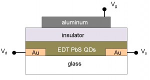
- Figure 1: Schematic of top-gate bottom-contact device structure.

-
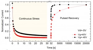
- Figure 2: Drain-source current during stress and recovery for a typical device.

- T. S. Mentzel, V. J. Porter, S. Geyer, K. MacLean, M. G. Bawendi, and M. A. Kastner, “Charge transport in PbSe nanocrystal arrays,” Physical Review Letters B, vol. 77, no. 7, pp. 075316, 2008. [↩]
- M. Law, J. M. Luther, Q. Song, B. K. Hughes, C. L. Perkins, and A. J. Nozik, “Structural, optical, and electrical properties of PbSe nanocrystal solids treated thermally or with simple amines,” Journal of the American Chemical Society, vol. 130, no. 18, pp. 5974-5985, 2008. [↩]
- J. M. Luther, M. Law, Q. Song, C. L. Perkins, M. C. Beard, and A. J. Nozik, “Structural, optical, and electrical properties of self-assembled films of PbSe nanocrystals treated with 1,2-ethanedithiol,” ACS Nano, vol. 2, no. 2, pp. 271-280, 2008. [↩]
- Y. Liu, M. Gibbs, J. Puthussery, S. Gaik, R. Ihly, H. W. Hillhouse, and M. Law, “Dependence of carrier mobility on nanocrystal size and ligand length in PbSe nanocrystal solids,” Nano Letters, vol. 10, no. 5, pp. 1960-1969, 2010. [↩]