Analog Front-end Design for Portable Ultrasound Systems
- Category: Circuits & Systems, Medical Electronics
- Tags: Anantha Chandrakasan, Bonnie Lam, Charles Sodini, Hae-Seung Lee, Kailiang Chen
The Capacitive Micromachined Ultrasound Transducer (CMUT) is an alternative to traditional piezoelectric transducers. The CMUT technology provides an opportunity for highly integrated ultrasound-imaging system solutions because of its CMOS compatibility, ease of large array fabrication, and improved bandwidth and sensitivity performance [1] .
This project aims to provide a highly flexible platform for 3D ultrasound imaging. Figure 1 presents the system architecture. The CMUT device is flip-chip bonded to the supporting electronic circuits, which eliminates the cables that are usually required by traditional systems between the piezoelectric transducers and circuits. As a result, the channel count of the imaging system is increased and the capacitive loading due to cables is greatly reduced.
The first prototype chip of the transmitter and receiver analog front-end for a 1D CMUT array is fabricated and is under testing. The block diagram of the implemented chip is shown in Figure 2. It contains four channels of independent transmitters and receiver chains. External control can be implemented for beamforming and Time-Gain Compensation (TGC). In each channel, the transmitter generates high voltage electric pulses to drive the CMUT device. A 3-level pulse shaping transmitter is designed to increase the transmitted signal power within the transducer bandwidth. The design uses MOS high voltage transistors for a pulse magnitude as large as 32 Vpp. The pulse frequency is programmable between 1~10 MHz and the pulse duration is programmable between about 0.5~20 us.
On the receiver side, a Low Noise Amplifier (LNA) implemented with a trans-impedance amplifier interfaces to the CMUT. The LNA is optimized for noise, power, and bandwidth trade-offs. The LNA can also be switched from “on” and “off” within 5 us. This switching saves system power when LNA is not needed. A Variable Gain Amplifier (VGA) follows the LNA to realize the Time-Gain Compensation function. Instead of a linear TGC profile, this VGA implements the TGC in a low power way, with discrete gain steps to compensate signal attenuation with coarse resolution. The VGA consumes 300 uA, and the gain setting can be changed in 6 dB per step with a tunable range of about 54 dB.
The prototyped chip is 3 mm X 3 mm in size. The simulated performance shows that each receive channel consumes 18.1 mW in normal mode and 1.7 mW in sleep mode. The programmable Rx gain range is from 152 dB to 99 dB at 3 MHz, with gain steps of 6 dB per step. The Rx Bandwidth is 6.0 MHz and the Rx Noise Figure is 11.3 dB within the signal bandwidth. The Tx pulsing energy efficiency is 38.2 nJ / pulse for an assumed 60 pF load from one CMUT element.
-
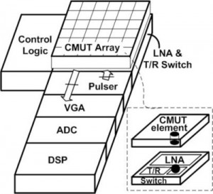
- Figure 1: The architecture of a 3D ultrasound imaging system with CMUT devices.

-
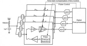
- Figure 2: The block diagram of the first prototype ultrasound analog front-end chip.

- O. Oralkan, “Acoustical imaging using capacitive micromachined ultrasonic transducer arrays: Devices, circuits, and systems,” Ph.D. dissertation, Stanford, Palo Alto, 2004. [↩]