Hole Mobility Enhancement in III-V FETs through Uniaxial Strain
- Category: Electronic Devices
- Tags: Jesus del Alamo, Ling Xia
In Si p-type metal-oxide-semiconductor field-effect transistors (MOSFETs), the incorporation of mechanical strain in the channel has greatly enhanced hole velocity and transistor performance. As conventional Si MOSFET scaling gets increasingly difficult, III-V FETs are receiving a great deal of attention for a future sub-10-nm complementary MOS (CMOS) logic technology. In fact, in some measure, n-channel III-V FETs have been found to outperform Si MOSFETs with gate lengths down to 30 nm. To complement these n-channel III-V FETs, we are investigating high-performance p-channel III-V FETs. Given that the hole mobility of most III-Vs is at best comparable to that of Si, strain is being investigated as a path to enhance the hole mobility and consequently III-V pFET performance. In our present work, we experimentally study the potential to improve p-channel III-V FETs by introducing uniaxial strain into these devices.
To introduce controlled uniaxial strain into FETs, we designed and fabricated a mechanical apparatus (Figure 1) to bend III-V chips. This apparatus allows the application of uniaxial strain up to ±0.3% to III-V chips. Electrical measurements on FETs can be performed while the chips are bent. In addition, Hall measurements can also be carried out by applying a magnetic field with a pair of permanent magnets. These allow the direct evaluation of strain effects on the hole mobility and hole concentration.
The structures we studied include p-channel FETs and ungated Hall bars based on InGaSb [1] , GaAs [2] and InGaAs [3] . The devices were either supplied by our collaborators or fabricated at MIT. Figure 2 shows an example of an InGaSb quantum-well FET (QW-FET) structure we have studied and its response to applied uniaxial stress [1] . As shown in the figure, stress significantly changes the operation of the device. In fact, we found that changes occur in the device drain current and threshold voltage. These changes are the manifestations of changes in hole mobility and hole concentration. The change in hole mobility shares similar physics with what has been found earlier in Si and Ge pFETs. The hole concentration change is due to the stress-induced piezoelectric field. The piezoelectric effect does not exist in Si or Ge FETs but is found to be important to consider in III-V FETs. The magnitude of stress-induced hole mobility enhancement in our III-V FETs has been found comparable to or even larger than those in Si and Ge pFETs. The maximum hole mobility change was found to be 12% per 100 MPa stress in a In0.24Ga0.76As quantum well, which is 70% higher than in Si p-MOSFETs. Our work suggests that uniaxial stress is a viable path to enhance hole mobility in high-performance p-channel III-V FETs.
-
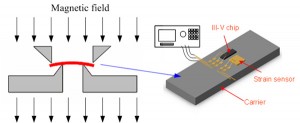
- Figure 1: Chip-bending apparatus to introduce uniaxial strain into III-V FETs. This setup allows repeatable electrical measurements with III-V chips stressed at various levels. In addition, Hall measurements can be conducted with a magnetic field applied.

-
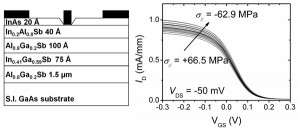
- Figure 2: (Left) The cross section of a p-channel In0.41Ga0.59Sb quantum-well FET (QW-FET). (Right) Measured transfer characteristics change of the QW-FET with <110> uniaxial stress applied by our mechanical apparatus.

- L. Xia, J. B. Boos, B. R. Bennett, M. G. Ancona, and J. A. del Alamo, “Hole mobility enhancement in In0.41Ga0.59Sb quantum-well field-effect transistors,” Applied Physics Letters, vol. 98, p. 053505, 2009. [↩] [↩]
- L. Xia, V. Tokranov, S. R. Oktyabrsky, and J. A. del Alamo, “Experimental study of <110> uniaxial stress effects on P-channel GaAs quantum-well FETs,” To be published on IEEE Transaction of Electron Devices. [↩]
- L. Xia, V. Tokranov, S. Oktyabrsky, and J. A. del Alamo, “Mobility enhancement of two-dimensional hole gas in an In0.24Ga0.76As quantum well by <110> uniaxial strain,” Proc. International Symposium of Compound Semiconductor, p. 396, 2011. [↩]