A Self-aligned Gate Technology for InGaAs Quantum-well Field-effect Transistors
- Category: Electronic Devices
- Tags: Jesus del Alamo, Taewoo Kim
As conventional Si CMOS scaling approaches the end of the roadmap, III-V based field-effect transistors appear as an increasingly viable alternative to continue transistor size scaling. A great deal of the excitement about the prospects of III-Vs comes from the excellent logic characteristics that have recently been demonstrated in InGaAs high electron mobility transistors (HEMTs) with gate length as small as 30 nm. While being quite far in structure from an ideal logic III-V MOSFET, the HEMT has been demonstrated to be an excellent model system to study fundamental device physics and technology issues. It also has provided well-calibrated and relatively parasitic-free device results to support the development of simulators that would allow us to chart the future of a III-V logic technology. In this regard, there is great value in continuing to push the scaling of HEMTs to explore significant device physics issues in the relevant dimensional range. Until now, the demonstrated HEMTs have had a quite large gate-source distance of around 1 mm and a source resistance of around 200 ohm-mm. These are large values compared with state-of-the-art Si CMOS technology. To address these deficiencies, a self-aligned gate scheme is essential.
Our group has been engaged in self-aligned gate technologies for III-V FETs for several years [1] [2] . In our first approach, W was used as non-alloyed ohmic contacts with the gate nested inside an opening in a self-aligned way. Through this technology, 90-nm gate length InGaAs HEMTs were demonstrated with LGS = 60 nm. This technology featured a simple lift-off gate with high parasitic capacitance. As a result, the frequency response of the fabricated transistors was unremarkable. In this work, we demonstrate a new self-aligned gate technology with non-alloyed Mo-based ohmic contacts and a very low parasitic capacitance gate design. The proposed device architecture allows for the incorporation of a high-K gate dielectric in the gate stack to achieve MOS-type devices. The new process delivers very low values of contact resistance and source resistance plus record high-frequency characteristics. We have obtained a contact resistance (Rc) of about 7 ohm-mm, which is a near-record result. The contact is thermally stable up to 600°C. Figure 1 shows STEM images of a fabricated Lg = 60-nm device. Figure 2 shows short-circuit current-gain cut-off frequency fT as a function of Lg for sub-100-nm InGaAs and InAs HEMTs. The obtained fT value in our device is the highest ever reported in a HEMT with a gate length above Lg = 50 nm and bodes well for the future scalability of this device design. This result strongly suggests a path towards the demonstration of III-V MOSFETS for future CMOS.
-
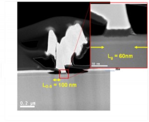
- Figure 1: Cross-section STEM images of Mo-based SAG HEMT with Lg = 60 nm with 100-nm gate-source contact separation.

-
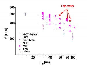
- Figure 2: The fT as a function of Lg for reported InGaAs and InAs HEMTs in the literature, including Mo-based SAG HEMTs in this work.
