Low Voltage Organic Semiconductor-based Devices and Circuits
- Category: Circuits & Systems, Electronic Devices
- Tags: Akintunde Akinwande, Melissa Smith
Organic semiconductor-based devices can easily be scaled to large areas and fabricated on flexible, elastic, and non-planar surfaces at low temperatures. These properties give rise to a myriad of applications from printable and flexible circuits, displays, and solar cells to artificial skin, neurons, and other biosensors; unattainable with traditional silicon electronics technologies [1] .
To enable new, exciting applications, a low voltage circuit technology is being developed. The device of interest is the pentacene-based organic thin-film transistor (OTFT). Currently, pentacene shows the most promise as an organic semiconductor given its relatively high carrier mobility and chemical stability. Delocalized π-bonded electrons enable p-type semiconducting behavior in pentacene [1] . To realize organic semiconductor-based devices as a pervasive complement to Si CMOS devices, the electrical performance of organic semiconductor devices must improve. This requirement demands that the operating voltage must reduce and carrier mobility increase while the device maintains a high current and on-current to off-current ratio, all of which must be reproducible. Ultimately, these device parameters are related to the semiconductor, the insulator, and the semiconductor/insulator interface quality (grain size, growth modes, material phases, interface states, trapped charges, roughness, etc.).
Insulator and semiconductor engineering are being explored as a means to improve performance and illustrate the potential of this technology for large area nanoelectronics. Conventional methods of device fabrication have been used to address performance issues with limited success. In this work, initial efforts will concentrate on engineering the gate insulator by using a high dielectric constant material. Specifically, BZN (Bi1.5Zn1 Nb1.5O7) is a paraelectric pyrochlore system that boasts a high dielectric constant, low dielectric loss, and low co-firing temperature, making it a viable insulator for improving OTFT performance and enabling advanced circuit design [2] . The performance of this BZN compared to parylene as an insulator is illustrated in Figures 1 and 2. Later phases of this work will focus on engineering the semiconductor deposition. Enhancements to standard evaporative deposition techniques will be explored by in situ coupling of new forms of energy to control pentacene thin-film morphology and defects.
-
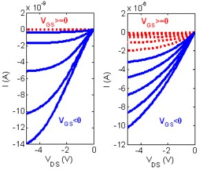
- Figure 1: Comparison of output characteristics of OTFTs with two different insulators, BZN (right) and BZN with a parylene surface treatment (left). VGS is stepped from 5 V to -5 V for both devices. Typical VT for BZN is ~2V. Treating the surface of the BZN with parylene shifts the VT to ~-0.5 V.
-
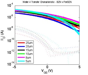
- Figure 2: Comparison of transfer characteristics of OTFTs with BZN, and BZN with parylene surface treatment with various channel lengths. VT for BZN is greater than 0 V (positive). VT for the BZN/parylene insulator stack is less than 0 V (negative). This is the foundation for inverter circuits.

- M. Kitamura and Y. Arakawa, “Pentacene-based organic field-effect transistors,” Journal of Physics-Condensed Matter, vol. 20, May 2008. [↩] [↩]
- Y. Choi, I. D. Kim, H. L. Tuller, and A. I. Akinwande, “Low-voltage organic transistors and depletion-load inverters with high-K pyrochlore BZN gate dielectric on polymer substrate,” IEEE Transactions on Electron Devices, vol. 52, pp. 2819-2824, Dec. 2005. [↩]