1.8-kV-breakdown AlGaN/GaN HEMT on Si Substrate
- Category: Electronic Devices
- Tags: Min Sun, Tomas Palacios
The combination of high critical electric field, carrier mobility and thermal stability makes GaN an ideal semiconductor for power switches [1] . Additionally, the growth of GaN-based semiconductors on large area Si substrates significantly reduces the cost of these devices and enables their fabrication in state-of-the-art Si fabs. This paper demonstrates a GaN-on-Si HEMT with a 1.8-kV breakdown voltage and a record 2.4 mΩ,cm-2. specific on resistance.
The devices were fabricated on an AlGaN/GaN heterostructure grown on a 4-in Si substrate by MOCVD. The fabrication process began with plasma etching for device isolation; then a Ti/Al/Ni/Au metal stack was deposited on the source and drain contact region, followed by an 870°C rapid thermal annealing to form the ohmic contacts. Two-micron-long gate electrodes were deposited using Ni/Au/Ni. The devices have a gate-to-source distance of 1.5 μm and gate width of 100 μm. The gate-to-drain distance L-gd. varies from 5 μm to 35 μm.
Breakdown voltage measurements were carried out at a gate voltage Vg.=−8 V and with the samples immersed in Fluorinert to avoid surface flashover through air. The breakdown voltage Vbr. was defined as the voltage when the drain-to-source leakage current density I-D. exceeded 1 mA/mm. The breakdown voltage of the devices increases linearly with Lgd at a rate of 140 V/μm (Figure 1). However, the breakdown voltage saturates at Lgd.=12 μm due to vertical leakage through the Si substrate [2] . The maximum current density for a device with Lgd=12 μm is 375 mA/mm. Figure 2 shows the specific on resistance of the devices fabricated in this work as a function of breakdown voltage. This performance makes these devices very promising for power electronic applications including electric vehicles and photo-voltaic power inverters. Even higher breakdown voltage could be achieved by removing the substrate [2] ; this goal is the focus of our on-going work.
-
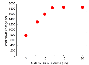
- Figure 1: Breakdown voltage Vbr as a function of Lgd.

-
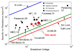
- Figure 2: versus breakdown voltage for AlGaN/GaN power transistors on different substrates.

- B. J. Baliga, “Power semiconductor device figure of merit for high-frequency applications,” Electron Device Letters, IEEE, vol. 10, no. 10, pp. 455-457. [↩]
- L. Bin and and T. Palacios. “High breakdown (>1500V) AlGaN/GaN HEMTs by substrate-transfer technology,” Electron Device Letters, IEEE, vol. 31, no. 9, pp. 951-953. [↩] [↩]