III-V and IV Semiconductors for Thermoelectric and Thermophotovoltaic Applications
- Category: Materials
- Tags: Adam Jandl, Eugene Fitzgerald
We are developing materials for thermoelectric and thermophotovoltaics applications. Our objective is to develop III-V and/or IV superlattices with low thermal conductivity and high electrical conductivity to maximize the thermoelectric figure of merit. Additionally, it may be possible to increase the Seebeck coefficient in these materials by introducing a narrow but large peak in the density of states near the Fermi energy. For our thermophotovoltaics research, we are investigating graded buffers of InAsP as a platform for the growth of low defect density InAsP, InGaAs, and GaAsSb tandem photovoltaic cells with band gap energies in the range of 0.6 eV to 0.8 eV.
Through our collaborations we have designed and created GaAs/AlAs superlattices (SL) to determine the method of phonon transport in semiconducting superlattices. Measurements by our collaborators have revealed that thermal transport may not be diffusive and further work is being done to investigate this transport. GaAs/Ge structures have also been grown but lack planar interfaces due to surface kinetics during growth. Future experiments will explore the growth of GaAs and Ge structures and determine the thermal and electrical transport properties in these systems. Figure 1 is a dark field cross-section TEM image of this sample.
Our work on thermophotovoltaics is two-pronged, with one focusing on minimizing threading dislocation densities (TDD) introduced by InAsP graded buffers and the other focusing on the growth and doping of InAsP and InGaAs pn-junctions with band gap energies in the range of 0.6 eV to 0.8 eV. Our work on InAsP graded buffers has focused on determining the relationship between the strain accumulation rate in the buffer and the resulting TDD in the active regions. The pn-junctions shown in Figure 2 targeted two compositions of InGaAs and one of InAsP to achieve the desired band gap energies.
-
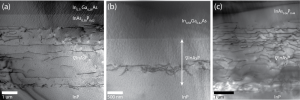
- Figure 1: Cross-sectional bright field <220> TEM images of InGaAs and InAsP pn-junctions. The band gap energy of the top- most layer of each structure is (a) 0.6 eV, (b) 0.7 eV, and (c) 0.8 eV.

-
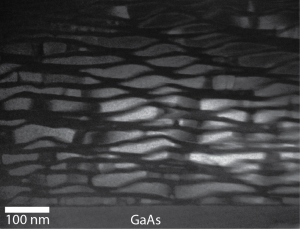
- Figure 2: Cross-section dark field TEM image of GaAs/Ge multilayer on GaAs (001) 6° offcut towards the nearest {111} plane. The bright regions in the film are GaAs, and the dark regions are Ge.
