A Self-aligned InGaAs Quantum-well Field-effect Transistor for Logic Applications
- Category: Electronic Devices
- Tags: Dimitri Antoniadis, Jesus del Alamo, Jianqiang Lin
InGaAs is a promising candidate for channel material for future high-performance CMOS logic applications because of its superior electron transport properties [1] . InGaAs quantum-well metal-oxide-semiconductor field-effect transistor (QW-MOSFET) research has recently attracted great interest from the IC device community. N-channel InGaAs-based High-electron-mobility transistors (HEMTs) fabricated previously at MIT have served as an excellent testbed with which to explore issues of importance in a future III-V CMOS technology. They demonstrated outstanding logic device characteristics due to the high injection velocity at low supply voltage and high electrostatic integrity afforded by the quantum-well channel [1] [2] [3] . These advantages, if ported over to InGaAs MOSFETs, can eventually lead to integrated circuits exhibiting high speed with reduced power dissipation.
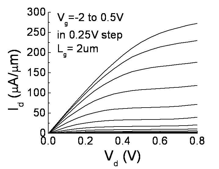
There are many challenges in the development of a InGaAs QW-MOSFET technology for future CMOS applications. For example, low series resistance and a compact footprint are required. In this work we prototype a novel self-aligned InGaAs QW-MOSFET that can address these problems. The cross-sectional schematic of the QW-MOSFET is shown in Figure 1. This device uses a thin Al2O3 gate dielectric. Molybdenum-based ohmic contacts are self-aligned to the gate. This self-alignment scheme reduces the spacing between the contacts and the gate and leads to a lower series resistance. A first working prototype QW-MOSFET with Lg =2 mm has been fabricated, and the output characteristics are shown in Figure 2. Process optimization, aimed at a further reduction in the source resistance, is being carried out. The scaling behavior and performance analysis with respect to silicon technology for this new device structure will be investigated.
-
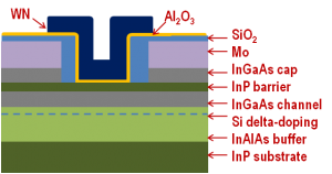
- Figure 1: Cross-sectional schematic of self-aligned InGaAs QW-MOSFET.

-
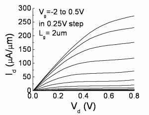
- Figure 2: Output characteristics of a prototype QW-MOSFET with Lg =2 μm.
- D.-H. Kim, J. A. del Alamo, D. A. Antoniadis, and B. Brar, “Extraction of virtual-source injection velocity in sub-100 nm III-V HFETs,” in IEDM Tech. Dig., pp. 861-864, Dec. 2009. [↩] [↩]
- D.-H. Kim and J. A. del Alamo, “30 nm E-mode InAs PHEMTs for THz and future logic applications,” in IEDM Tech. Dig., pp. 719-722, Dec. 2008 [↩]
- T.-W., Kim, D.-H. Kim, and J. A. del Alamo, “Logic characteristics of 40 nm thin-channel InAs HEMTs,” 22nd International Conference on Indium Phosphide and Related Materials, pp. 496-499, May 2010. [↩]