GaN High Frequency Transistors
- Category: Electronic Devices
- Tags: Dong Seup Lee, Tomas Palacios
GaN-based high electron mobility transistors (HEMTs) have great potential for high power/frequency applications due to their outstanding combination of large breakdown voltage and high electron velocity. Among the different possible nitride structures, InAlN/GaN heterostructures have attracted much attention recently because they enable an extremely high charge density with a thin barrier thickness [1] . With the use of these advantages, outstanding progress in the frequency performance of InAlN/GaN transistors has been recently achieved. Sun et al. reported a 55-nm gate length device with fT of 205 GHz (fmax = 191 GHz) [2] and Lee et al. demonstrated a 30-nm gate length device with fT of 245 GHz [3] .
In this study, we used an AlGaN back-barrier in InAlN/GaN HEMT structures for the first time and studied its impact on the DC and RF characteristics of these devices [4] . A maximum drain current of 1.49 A/mm is obtained at Vgs=2 V in the device with the back-barrier, about 27 % lower than that of the standard device (2.05 A/mm at Vgs=2 V). The smaller drain current in the device with the back-barrier mainly results from the lower sheet charge density and subsequent higher threshold voltage. However, the output conductance is significantly smaller in the device with the back-barrier, which shows an effective suppression of the short-channel effects. In addition, in sub-100-nm-gate-length transistors, the back-barrier makes it possible to maintain a drain-induced barrier lowering (DIBL) near 50-60 mV/V while preventing the degradation of the subthreshold swing (SS). Thanks to the reduced short-channel effects, 65-nm-gate-length devices with a back-barrier showed an fT of 210 GHz, which is higher than that of the standard device with the same gate length (195 GHz). Moreover, in a sub-30-nm-gate-length device with AlGaN back-barrier, an fT of 270 GHz, the highest fT ever reported in GaN transistors, was achieved.
-
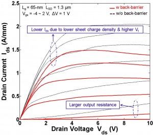
- Figure 1: Output characteristics of InAlN/GaN HEMTs (Lg = 65-nm) with and without an AlGaN back-barrier.

-
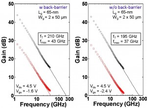
- Figure 2: RF performance of the 65-nm-gate-length InAlN/GaN HEMTs (a) with and (b) without the AlGaN back-barrier.

- J. Kuzmik, “Power electronics on InAlN/(In)GaN: Prospect for a record performance,” IEEE Electron Device Lett. vol. 22, no. 11, pp. 510-512, Nov. 2001. [↩]
- H. Sun, A. R. Alt, H. Benedickter, E. Feltin, J.-F. Carlin, M. Gonschorek, N. Grandjean, and C. R. Bolognesi, “205-GHz (Al, In)N/GaN HEMTs,” IEEE Electron Device Lett., vol. 31, no. 9, pp. 957-959, Sep. 2010. [↩]
- D. S. Lee, J. W. Chung, H. Wang, X. Gao, S. Guo, P. Fay, and T. Palacios, “245 GHz InAlN/GaN HEMTs with oxygen plasma treatment,” IEEE Electron Device Lett., vol. 32, no.6, pp.755-757, Jun. 2011. [↩]
- D. Lee, X. Gao, S. Guo, and T. Palacios, “InAlN/GaN HEMTs with AlGaN back-barriers,” IEEE Electron Device Lett., vol. 32, no. 5, pp.-617-619, May 2011. [↩]