CNT-based Optoelectronic Device Packaging
- Category: Nanotechnology, Optics & Photonics
- Tags: Rajeev Ram, San-Liang Lee
Carbon nanotubes (CNTs) are excellent heat spreaders for packaging electronic/photonic devices due to their high thermal conductivity and good mechanical strength [1] [2] . They have been used for packaging LED chips [3] [4] [5] . However, poor adhesion between CNTs and adjacent materials may impact device yield and reliability. We proposed a platform for optoelectronic device packaging by integrating vertical aligned CNTs (VACNTs) onto patterned silicon U-grooves for achieving enhanced thermal conduction and stable mechanical properties.
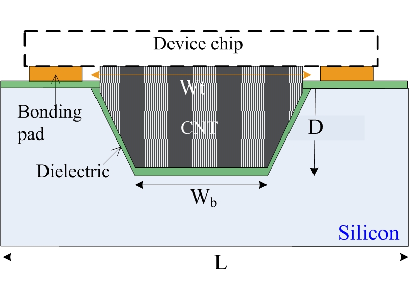
Figure 1 shows the schematic of the CNT-based platform. CNTs are grown on a silicon trench to provide heat spreading for the bonded device chip. A thin dielectric layer between CNTs and silicon substrate is usually needed to eliminate current leakage to the substrate. The device chip is bonded to the platform by the bonding pads on chip surface. Figure 2 shows the calculated thermal resistance of the CNT platform by using the Finite Element Method. A silicon monoxide (SiO) film of 500-nm thick is used as the dielectric layer. The planar silicon platform with the same thickness of SiO is also simulated for comparisons. When the top open area of the U-groove covers about 87% of the device chip and the depth is about 30% of the 200-mm thick silicon substrate, the CNT platform can provide about 39% reduction in thermal resistance if the thermal conductivity of CNTs is 600 W/mK. The reduction can reach about 50% by using a deeper U-groove with taller CNTs. The enhancement on the thermal conduction by the CNT platform results not only from the use of high-thermal-conductivity VACNTs but also from the increased surface area of the low-thermal-conductance dielectric layer.
The CNT platforms were demonstrated for packaging red LEDs to have high saturation current and high manufacturing yield [6] .
-
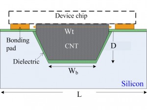
- Figure 1: Cross-sectional view of device packaging using a CNT-based platform.
-
- Figure 2: Simulated thermal resistance versus the top open surface area of the U-groove for growing CNTs. The thermal resistance is normalized to the thermal resistance of the silicon substrate with a 500-nm thick silicon monoxide layer on the surface, 12.9 K/W. The surface area is normalized to the area of heat source, 300µm by 300 µm. The depth is normalized to the thickness of silicon substrate, 200µm.
- S. Berber, Y. K. Kwon, and D. Tomanek, “Unusually high thermal conductivity of carbon nanotubes,” Phys. Rev. Lett., vol. 84, pp. 4613-4616, 2000. [↩]
- P. Kim, L. Shi, A. Majumdar, and P. L. McEuen, “Thermal transport measurements of individual multiwalled nanotubes,” Phys. Rev. Lett., vol. 87, pp. 215502-215505, 2001. [↩]
- K. Zhang, G. W. Xiao, C. K. Y. Wong, H. W. Gu, M. M. F. Yuen, P. C. H. Chan, and B. Xu, “Study on thermal interface material with carbon nanotubes and carbon black in high-brightness LED packaging with flip-chip technology,” Proc. 55th IEEE Electronic Components and Technology Conference, pp. 60-65, Lake Buena Vista, FL, May 2005. [↩]
- K. Zhang, Y. Chai, M. M. F. Yuen, D. G. W. Xiao, and P. C. H. Chan, “Carbon nanotube thermal interface material for high-brightness light-emitting diode cooling,” Nanotechnology, vol. 19, pp. 215706-215714, 2008. [↩]
- M. Arik, S. E. Weaver, Jr., J. C. Carnahan, C. A. Becker, W. D. Gerstler, “Electronic devices and methods for making same using nanotube regions to assist in thermal heat-sinking,” US Patent, 6864571, Mar. 8, 2005. [↩]
- S.-C. Chen, S.-L. Lee, H. Lo, Y.-J. Hung, K.-Y., Lee, C.-G. Tu, Y.-T. Pan, and R. J. Ram, “VACNT-on-silicon platform for improving heat conduction in optoelectronic packaging,” in Proc. Conference on Lasers and Electro-Optics (CLEO), Baltimore, MD., May 2011. [↩]