Energy-delay Trade-off for Devices with Asymmetric n-type and p-type Current Drives from a Static-CMOS Circuit-level Perspective
- Category: Circuits & Systems, Electronic Devices
- Tags: Dimitri Antoniadis, Lan Wei
Historically, digital logic devices are benchmarked by the on-state current (Ion) at specified off-state current (Ioff) and supply voltage (Vdd) at each technology node. Emerging device technologies are often targeted to outperform Si MOSFETs at the same Ioff and Vdd. Some emerging technologies, such as III-V transistors and Ge transistors, have great advantages in either n-type or p-type devices, instead of both types, at the device level in terms of Ion. However, recent work [1] shows that devices optimized based on the conventional device-level Ion methodology may not necessarily give the best performance at the circuit-level. In this work, we extend the methodology proposed in [1] to study the technologies with asymmetric n-type and p-type driving capabilities from a circuit-level perspective.
Circuit-level delay and energy are calculated following the strategies described in [1] , assuming static CMOS logic gates. The smaller of the widths of nMOS (Wn) and pMOS (Wp) is fixed to be 1 mm. Assuming the same pull-up and pull-down delay, the P/N ratio (k=Wp/Wn), is adjusted according to the on-current. Figure 1(a) minimizes energy per switch at each delay point for selected P/N ratio, with a pMOS and nMOS transporting 10x and 1x current of the 11-nm projection device in [1] at the same bias. The corresponding dynamic energy (Edyn) over total energy (Etot) is shown in Figure 1(b). It is shown that the optimal sizing ratio is not necessarily 1/10 as in following the conventional sizing scheme. In fact, the optimal k is the smallest number that can maintain Edyn at around 80% of Etot. As Figure 2 shows, compared with the baseline technology with symmetric nMOS and pMOS, the technology that improves the transport capability of only one type of devices hardly benefits the circuit-level energy-delay trade-off.
-
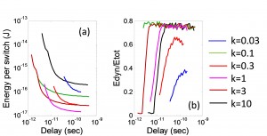
- Figure 1: (a) Minimum energy per switch and the corresponding (b) Edyn/Etot for a circuit application, assuming static-CMOS logic, with a logic depth of 20 and activity factor of 0.01, at selected P/N ratios. The pMOS and nMOS transporting 10x and 1x current of the 11-nm projection device in [1] at the same bias. When the penalty of static leakage power, which is proportional to Ioff, increases to assure the driving speed, i.e., Edyn/Etot decreases to be much less than 80%, the size of the weaker transistor should be increased to suppress the penalty.

-
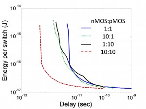
- Figure 2: The minimum energy per switch as a function of delay, with k as a free variable, for technologies with different strengths of nMOS and pMOS with the 11-nm ITRS projection in [1] as the nominal technology.

- L. Wei, S. Oh, and H. –S. Philip Wong, “Performance benchmarks for Si, III-V, TFET, and carbon nanotube FET – Re-thinking the technology assessment methodology for complementary logic applications,” 2010 IEEE International Electron Devices Meeting, pp. 16.2.1-16.2.4, San Francisco, CA, Dec. 2010 [↩] [↩] [↩] [↩] [↩]