High Voltage Degradation of GaN HEMTs for Power-switching Applications
- Category: Electronic Devices
- Tags: Donghyun Jin, Jesus del Alamo
The GaN high-electron-mobility transistor (HEMT) is a very promising device for power-switching applications due to the outstanding material properties of GaN such as high band-gap (3.4 eV) and high breakdown electric field (> 3×10⁶ V/cm), which enable these devices to achieve a very high breakdown voltage. However, the wide deployment of GaN HEMT technology is limited mostly by its electrical reliability. The lack of a native substrate for GaN epitaxial growth (SiC or Si are mostly used) means that a large density of mismatch defects might be present in the active device area, potentially introducing carrier trapping and compromising its electrical reliability. Trapping, in particular, is a significant problem in high-voltage switching devices. When the device is biased at a high blocking voltage in the OFF-state, electron trapping takes places over a large volume of the semiconductor. This trapping can cause a large increase of the on-resistance (RON) or a subsequent drain current drop. This problem is known as dynamic RON, or current collapse phenomenon [1] , which is one of the most prevalent degradation issues in GaN HEMTs. A high electric field in the OFF-state also induces a large amount of mechanical stress and above a certain critical value, crystallographic defects are formed which result in further enhanced electron trapping and subsequent current collapse [2] . These unique reliability issues are the key hurdle for the commercialization of this new disruptive technology.
Our research focuses mainly on the electrical reliability of GaN HEMTs specially designed for high voltage operation up to 200 V. Our systematic characterization experiments extract important figures of merits such as linear drain current (IDlin), gate leakage current in the OFF state (IGoff), drain resistance (RD), source resistance (RS) and threshold voltage (VT) as a device is being degraded. Figures 1 and 2 show the time evolution of IDlin, RD and RS in a step-stress-recovery experiment in the OFF-state at room temperature. A 5-min stress period is followed by 5-min recovery period under microscope light illumination. For each stress period, VGS= -5 V and VDS is incremented from 30 V to 150 V in 30-V steps. During the stress periods, IDlin/RD decreases/increases as VDS stress voltage goes up to 90 V. Above 90 V, however, the degradation in IDlin and RD is mitigated. During the recovery periods under visible light, IDlin and RD fully recover back to the original value before the stress. These results support a hypothesis in which trapping and detrapping are taking place during the stress and recovery periods, but no permanent damage is being introduced. From separate experiments we have learned that the traps involved are all native traps; that is, no new traps are being created as a result of high-voltage stress. Since these trapping and detrapping dynamics are most relevant in determining dynamic RON during the high frequency switching operation, a precise understanding of this behavior under high voltage stress in a much shorter time scale is of great importance.
-
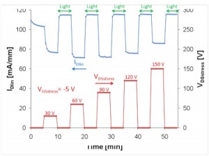
- Figure 1: Time evolution of IDlin and stress voltage (VDSstress) in a step-stress-recovery experiment in the OFF-state in GaN HEMTs. VDS is step stressed from 30 V to 150 V in 30-V steps and 5-min stress periods. A 5-min recovery period under visible light illumination follows each stress period. Trapping is evident but no permanent IDlin degradation is observed.

-
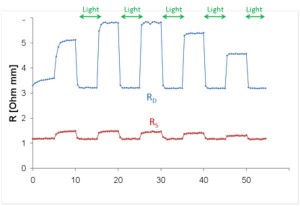
- Figure 2: Time evolution of RD and RS in the step-stress-recovery experiment of Figure 1. The full recovery of RD and RS indicates trapping effects that involve only native traps.

- J. A. del Alamo and J. Joh, “GaN HEMT reliability,” Microelectronics Reliability, vol. 49, pp. 1200-1206, 2009. [↩]
- J. Joh and J. A. del Alamo, “Impact of electrical degradation on trapping characteristics of GaN high electron mobility transistors,” International Electron Devices Meeting Technical Digest, pp. 461-464, Dec. 2008. [↩]