Nano-scale Metal Contacts for Future III-V CMOS
- Category: Electronic Devices, Materials, Nanotechnology
- Tags: Alex Guo, Jesus del Alamo

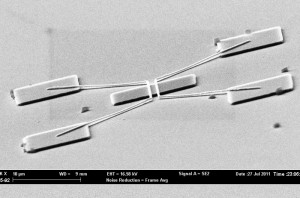
Figure 1: Cross section image of a nano-TLM structure. Metal line with contact length 230nm and spacing 780nm was observed after ebeam lithography, metal lift-off and mesa etching steps. Image was taken using Zeiss Supra-40 scanning electron microscope.
The scaling of MOSFETs in recent years has pushed the gate length down to less than 20 nanometers. Further gate length scaling is extremely challenging due to worsened short channel effects at the nanometer scale. Recently, much effort has been put into new device materials and structures to extend scaling trend for several more generations. Among others, III-V CMOS has shown promising results. One of the key elements for a high performance, small footprint III-V CMOS technology is a nanometer scale metal contact with low contact resistance. This study focuses on developing such a contact. To help us better understand ohmic contact properties in the quantum regime, this study explores the contact properties of Mo-based metallization on a III-V semiconductor substrate in the nanometer scale. The goals of the project are to develop a fabrication process that will produce good ohmic contact down to 50-nm contact length and to study the metal contact characteristics in the quantum regime.
Our approach consists on fabricating a nano-TLM (transmission line model) structure. The key step in this is defining thin metal lines using e-beam lithography technique. A Mo/Ti/Au contact is then e-beam evaporated. A lift-off process will follow to form nanometer scale metal lines and contacts. For device characterization, four 150-µm by 150-µm contact pads are designed to overlay on top of the metal lines to evaluate the contact resistance using Kelvin-type TLM measurements. Figure 1 shows the preliminary result of metal lines with 230nm contact length and a spacing of 780nm. The undercut defined the mesa width and the contact width of these metal lines. In the near future we expect to adapt nano-scale ohmic contact into III-V MOSFETs process, which will reduce the chip’s footprint and provide insight into the contact characteristics in the quantum regime.