Valence Band Offset Extraction Between Strained-Si and Strained-Ge Layers
- Category: Electronic Devices
- Tags: Dimitri Antoniadis, James Teherani, Judy Hoyt
The type-II band alignment between strained-silicon (s-Si) and strained-germanium (s-Ge) has been proposed for use in tunneling transistors due to the small effective band gap between the s-Si conduction band and s-Ge valence band [1] . The small effective band gap may substantially increase tunneling current compared to a Ge homostructure while maintaining low off-state leakage. However, the valence band alignment between thin layers of s-Si and s-Ge on a relaxed SiGe substrate has not been experimentally extracted.
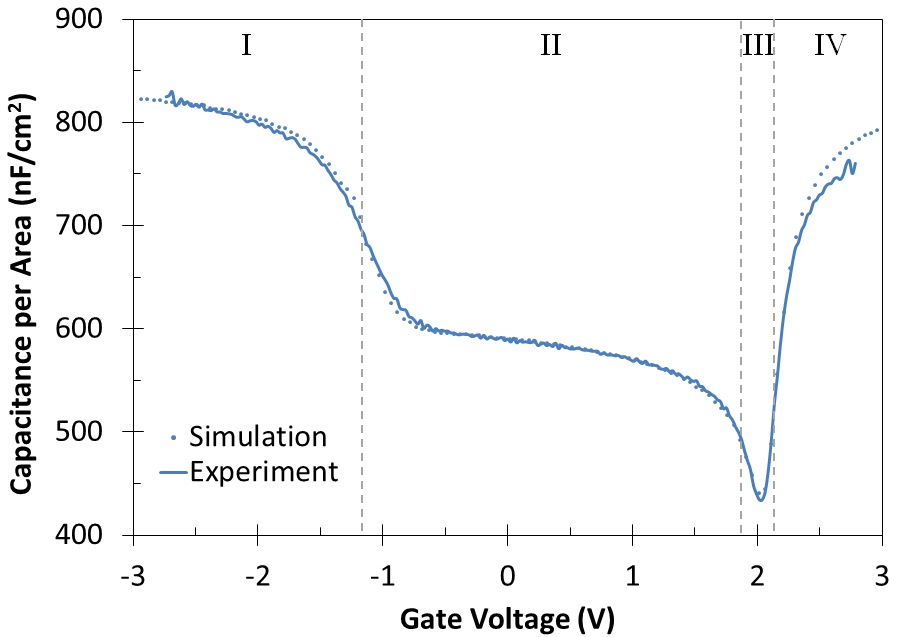
The experimental device structure consists of an Al2O3 high-κ dielectric (~6 nm) on a Si capping layer (~ 6 nm) on s-Ge (~ 6 nm) grown pseudomorphically on a relaxed SiGe buffer (~1 µm) with 40% Ge concentration. The wafers were processed into MOS-capacitors and measured using low-frequency and quasistatic C-V techniques. The valence band offset can be extracted by fitting the simulation data to experimental C-V measurements [2] . In Figure 1, the width of region II is dependent on the valence band offset and effective band gap between the s-Si and s-Ge layers.
Figure 2 shows the band structure and hole density as a function of position for the fabricated structure. At 0 V gate voltage, most holes near the surface of the capacitor are contained in the s-Ge quantum well. Since the s-Ge quantum well is displaced from the Al2O3 surface by the s-Si layer, the effective thickness is larger and thus the measured capacitance is lower than the oxide capacitance. As a more negative bias is applied to the gate, holes begin to accumulate at the s-Si/Al2O3 surface so that the total capacitance increases and approaches the oxide capacitance. The extracted valence band offset between the s-Si and s-Ge layers was 740±30 meV, which also suggests a small effective band gap.
-

- Figure 1: C-V curve of experimental and simulation data of the structure shown in Figure 2. The simulation data is fitted by adjusting the valence offset and effective band gap between the s-Si and s-Ge layers. Regions I, II, III, and IV correspond to hole accumulation in the s-Si, hole accumulation in the s-Ge, hole depletion from the s-Ge, and electron inversion in the s-Si, respectively.
-
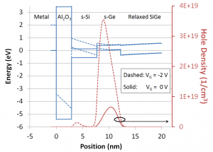
- Figure 2: The blue lines represent the band structure, and the red lines indicate the hole density as a function of position for the fabricated devices. The dashed lines show values at VG = -2 V, and solid lines show values at VG = 0 V. The text labels at the top of the plot indicate the different materials

- O. M. Nayfeh, C. N. Chleirigh, J. Hennessy, L. Gomez, J. L. Hoyt, and D. A. Antoniadis, “Design of tunneling field-effect transistors using strained-silicon/strained-germanium Type-II staggered heterojunctions,” IEEE Electron Device Letters, vol. 29, no. 9, pp. 1074-1077, Sep. 2008. [↩]
- C. N. Chleirigh, C. Jungemann, J. Jung, O. O. Olubuyide, and J. L. Hoyt, “Extraction of band offsets in strained Si/strained Si1-yGey on relaxed Si1-xGex dual-channel enhanced mobility structures,” in Proc. Electrochemical Society: SiGe: Materials, Processing and Devices, pp. 99–109, 2005. [↩]