GaN for Low Voltage Power Electronics
- Category: Electronic Devices
- Tags: Daniel Piedra, Tomas Palacios
GaN-based transistors have outstanding properties for the development of ultra-high efficiency and compact power electronics. The high electron mobility in the two-dimensional electron gas and the high critical electric field (greater than 10 times that of Si) make GaN high electron mobility transistors (HEMTs) ideal for power transistors [1] . This work focuses on developing devices for operation below 200V. We have developed a process to fabricate multi-finger AlGaN/GaN transistors with gate width of 39.6 mm (shown in Figure 1) that exhibit low on-resistance.
In addition to use in AlGaN/GaN HEMTs, the new technology has also been applied to InAlN/GaN devices. By using InAlN as the barrier material, we take advantage of the high sheet charge density (Ns=2.5×1013 cm-2) caused by higher polarization and reduced defect density of lattice-match InAlN barrier [2] . The high sheet charge density results in low sheet resistance and high current density, which are ideal for low-loss, efficient power switches. These devices have high breakdown voltage and excellent thermal stability due to the use of SiC substrates. Additionally, our group has developed gold- free GaN transistor technology using ohmic recess and a Ti/Al/W metallization. This technology is promising for the integration of GaN with silicon devices.
-
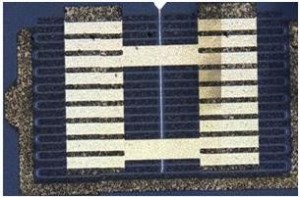
- Figure 1: AlGaN/GaN multifinger HEMT with Wg=39.6 mm.

-

- Figure 2: InAlN/GaN HEMT with varying gate widths.
- U. Mishra, L. Shen, T. Kazior, and Y. Wu, “GaN-based RF power devices and amplifiers,” Proc. IEEE, vol. 96, no. 2, Feb. 2008. [↩]
- F. Medjdoub, J.-F. Carlin, M. Gonschorek, E. Feltin, M. A. Py, D. Ducatteau, C. Gaquiére, N. Grandjean, and E. Kohn, “Can InAlN/GaN be an alternative to high power/ high temperature AlGaN/GaN devices?” Proc. IEDM Tech. Dig, 2006, pp. 927-930. [↩]