Hole Mobility in Strained-Ge p-MOSFETs with High-k/Metal Gate Stack
- Category: Electronic Devices
- Tags: Dimitri Antoniadis, Evelina Polyzoeva, Judy Hoyt
The need for high speed and density in modern integrated circuits requires new MOSFET channel materials, techniques for improved carrier transport, and continuous scaling of the device dimensions. Strained-Ge is implemented in this work as a material for enhanced hole transport. A high-k dielectric and metal gate stack is used for improved electrostatic control. At present, incorporating an epitaxial Si capping layer between the high-k dielectric and the Ge is the most promising approach for achieving a high quality Ge-dielectric interface, with 10x hole mobility enhancement relative to Si control devices reported for p-MOSFETs using this approach [1] . However, the use of a Si-cap leads to increased Capacitance Equivalent Thickness (CET) of the structure, which degrades electrostatic control. In addition, a Si cap provides a parasitic path for hole transport, which can deteriorate the effective hole mobility of the device at high inversion charge densities. Therefore, a process to fabricate MOSFETs by depositing a high-k dielectric directly on strained-Ge substrate should be developed and is the aim of this research.
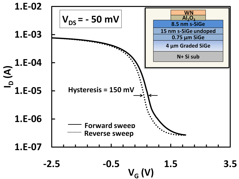
Strained-Ge MOSFETs with and without a Si-cap were fabricated to quantitatively assess the hole mobility and its dependence on dielectric interface quality. The gate stack for all the devices was 6-nm Al2O3/30 nm WN. Figure 1 shows the I-V characteristics of a strained-Ge MOSFET without a Si cap with the device cross-section shown in the inset. A very respectable on-to-off ratio is demonstrated for this long-channel (20-µm) device. Figure 2 shows the hole mobility for the devices with and without a silicon cap, compared to the universal mobility and previous results reported by Weber et al [2] . The samples without a silicon cap showed relatively high hysteresis (~150 mV) and lower hole mobility than the Si-capped devices. However, the mobility enhancement observed for the sample without the Si cap is larger than reported values for relaxed or strained Ge without a Si cap [3] [4] . This result is promising and illustrates the need for continued investigation of methods for improved passivation of the strained-Ge surface prior to direct high-k dielectric deposition.
-
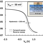
- Figure 1: I-V characteristics of a strained-Ge MOSFET without a silicon cap showing 200-mV hysteresis, suggesting some trapping mechanism still exists in the dielectric. The inset shows the cross-section of the device.
-
- Figure 2: Extracted hole mobility for the strained-Ge devices with and without Si cap. The enhancement factor compared to universal hole mobility curve is shown in the figure. The mobility of a previously reported device with a structure 3nm Si/7nm Ge and a HfO2/TiN gate stack is also shown for reference.

- M. L. Lee and E. A. Fitzgerald, “Optimized strained Si/strained ge dual-channel heterostructures for high mobility P- and N-MOSFETs,” IEDM Technical Digest, vol. 18, no. 1, pp. 1-4, 2003. [↩]
- O. Weber, Y. Bogumilowicz, T. Ernst, J.-M. Hartmann, F. Ducroquet, F. Andrieu, C. Dupre, L. Clavelier, C. Le Royer, N. Cherkashin, M. Hytch, D. Rouchon, H. Dansas, A.-M. Papon, V. Carron, C. Tabone, and S. Deleonibus, “Strained Si and Ge MOSFETs with high-k/metal gate stack for high mobility dual channel CMOS,” in Electron Devices Meeting, 2005, pp. 137-140. [↩]
- A. Ritenour, S. Yu, M. L. Lee, N. Lu, W. Bai, A. Pitera, E. A. Fitzgerald, D. L. Kwong, and D. A. Antoniadis, “Epitaxial strained germanium p-MOSFETs with HfO2 gate dielectric and TaN gate electrode,” IEDM ’03 Technical Digest, vol. 18, no. 2., pp. 1-4. [↩]
- J. Hennessy, “High mobility germanium MOSFETs: Study of ozone surface passivation and n-type dopant channel implants combined with ALD dielectrics,” Ph.D. Thesis, MIT, Cambridge, 2010. [↩]