CMOS Photonics
- Category: Optics & Photonics
- Tags: Jason Orcutt, Rajeev Ram

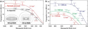
Figure 1: (a) Propagation loss as a function of waveguide width for wafers with and without thermal processing representative of the full electronics process. Solid fit lines estimating the confinement factor scaling for the indicated bulk material losses overlay measured data points. Inset of electric field contours show confinement change from core to cladding material for narrow waveguide widths. (b) Propagation loss as a function of wavelength and waveguide width for the thermally processed wafer.
Low propagation loss deposited waveguides are an important component to enable photonic integration in the majority of high-volume electronics processes. Polycrystalline silicon waveguides are desirable in this role as propagation losses below 10 dB/cm are achievable [1] [2] [3] using materials already common in such processes. However, previous demonstrations of low-loss poly-Si waveguides have utilized layer thicknesses of 200 nm or greater and reduced index-contrast oxynitride claddings to achieve such results. Further, the low-loss performance was not verified to withstand the high-temperature steps present in electronics processes.
To provide a suitable process integration test platform, 120-nm thick poly-Si waveguides were deposited and patterned on 300- mm wafers within the surrounding dielectric stack-up of a state-of-the-art memory process. To measure the impact of the thermal processing, the wafers were split with and without the all of the high-temperature anneals present in the full process for comparison. To minimize the impact of this thermal processing on top surface roughness, the waveguide core was first deposited at low-temperature by LPCVD to form an amorphous film and crystallized to form poly-Si with a ~950 °C 20-second anneal.
To measure the resulting waveguide loss, “paperclip” structures were patterned in which straight waveguide sections of varying propagation lengths are connected by identical input and output bends and vertical grating couplers. The resulting losses at 1550 nm as a function of waveguide width for wafers with and without thermal processing are shown in Figure 1a and are shown as a function of wavelength for the thermally processed wafers in Figure 1b. Although the waveguide loss increases slightly after thermal processing, both the as-deposited and end-of-line waveguide losses are below 10 dB/cm for 350-nm waveguide widths at 1550 nm. The narrow waveguides enable long-distance, on-chip routing to be enabled with 6.2 dB/cm loss.
- L. Liao et al., “Optical transmission losses in polycrystalline silicon strip waveguides: effects of waveguide dimensions, thermal treatment, hydrogen passivation, and wavelength,” J. Electron. Mater. vol. 29, pp. 1380-1386, 2000. [↩]
- Q. Fang et al., “Low loss (~6.45 dB/cm) sub-micron polycrystalline silicon waveguide integrated with efficient SiON waveguide coupler,” Opt. Express, vol. 16, pp. 6425-6432, 2008. [↩]
- C. W. Holzwarth et al., “Localized substrate removal technique enabling strong-confinement microphotonics in bulk Si CMOS processes,” in Conference on Lasers and Electro-Optics, Technical Digest (Optical Society of America, 2008), paper CThKK5. [↩]