Uniaxial Strained Ge for Non-planar p-MOSFETs
- Category: Electronic Devices
- Tags: Judy Hoyt, Pouya Hashemi, Winston Chern
Uniaxial strained Ge “nanobars” are of interest for future sub-10-nm gate length p-MOSFETs because of the excellent electrostatic control afforded by the non-planar device geometry and the potential for high hole velocity in the uniaxial strained Ge. This work investigates the fabrication technology for uniaxial strained Ge structures. The basic approach is to pattern a biaxially strained Ge epitaxial layer grown on a relaxed SiGe substrate into a narrow nanobar. The free surfaces of the nanobar sidewalls allow for the elastic relaxation of the lattice strain in the direction transverse to the bar, while maintaining the strain in the longitudinal direction [1] . Figure 1 shows a simulation of this effect, for 11-nm-thick strained Ge grown on relaxed SiGe after patterning into a 26-nm-wide nanobar. Figure 2 shows experimental results illustrating this concept. Raman spectroscopy was used to measure the amount of strain in the Ge nanobars for various widths that were patterned by e-beam lithography. The Raman data is consistent with lateral relaxation and shows that the strain approaches the uniaxial limit for ~ 20-nm-wide bars. These results are promising for the fabrication of future tri-gate type p-MOSFETs with improved transport properties.
-
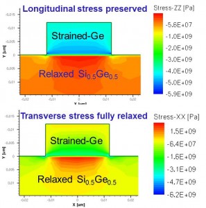
- Figure 1: Sentaurus simulation of strain relaxation of a strained Ge nanobar on a Si0.5Ge0.5 virtual substrate. The transverse strain is minimal on the surface of the nanobar while longitudinal stress is maintained.

-
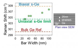
- Figure 2: Measured Raman shift of the Ge-Ge mode as a function of bar width for 11-nm-thick strained Ge epitaxial layer on a relaxed Si0.5Ge0.5 substrate. The uniaxial s-Ge limit, estimated to be half of the biaxial Raman shift, is shown for reference

- P. Hashemi, L. Gomez, M. D. Robertson, M. Canonico, and J. L. Hoyt, “Asymmetric strain in nanoscale patterned strained-Si/strained-Ge/strained-Si heterostructures on insulator,” Applied Physics Letters, vol. 90, no. 8, pp. 083109, Aug. 2007. [↩]