Scanning-neon and Helium-ion-beam Lithography
- Category: Materials, Nanotechnology
- Tags: Donald Winston, Karl Berggren, Vitor Manfrinato
A commercially-available scanning-helium-ion microscope of high source brightness [1] has been modified for operation with neon gas. This neon system had been evaluated for nano-machining [2] , but not for resist-based lithography, as has been done with helium systems [3] [4] . The neon system may enable a lithography process with higher resolution than any scanning-particle system to date. This possibility is due to the combination of the high-brightness source and the expected reduction of secondary-electron (SE) range relative to electrons or helium ions. In addition, the expected increase in SE yield relative to electrons or helium ions may lead to a lithography process with high sensitivity. This high sensitivity could allow critical doses below substrate-damage thresholds. Figure 1 presents preliminary data on the point-spread function (PSF) of neon compared to helium.
The Stopping and Range of Ions in Matter (SRIM) is a popular, industry-standard tool for simulating the trajectories of incident ions in a target sample. However, SRIM does not simulate the trajectories of secondary electrons (SEs) produced by ion-sample interactions. SEs are responsible for exposure of resist and thus figure prominently in modeling of electron-beam lithography and proton-beam lithography. We developed a hybrid approach to modeling helium-ion lithography that combines the power and ease-of-use of SRIM with the results of recent work simulating SE yield in helium-ion microscopy [5] . This approach traces along SRIM-produced helium-ion trajectories, generating and simulating trajectories for these SEs using a Monte Carlo method. Figure 2 illustrates the utility of our software, which can also simulate electron beams.
-
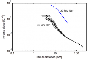
- Figure 1: Comparison of inverse dose versus measured feature half-width, which is the radial distance to the threshold for exposure, for 20 keV Ne+ and 30 keV He+, in thin (< 20 nm) HSQ on Si. We see from this plot that the neon beam is somewhat broader and also requires lower doses to achieve exposure.

-
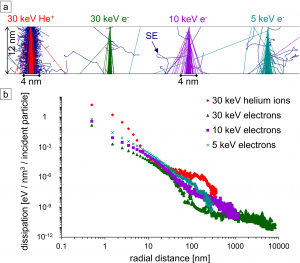
- Figure 2: (a) Projection plot of trajectories for incident particles and their SEs, for helium-ion and electron beams, in 12-nm-thick HSQ on Si. To reduce calculation time and to focus attention on the short-range effects on feature size such as forward scattering and SE range, the Si layer is a 36-nm-thick membrane rather than a bulk substrate. The image is cropped at the base of the resist layer for clarity. (b) Simulated PSFs in 12-nm-thick HSQ on bulk Si for each of the four beams in (a): 30 keV He+ (diamonds), 30 keV e- (triangles), 10 keV e- (squares), and 5 keV e- (x’s).

- B. W. Ward, J. A. Notte, and N. P. Economou, “Helium ion microscope: a new tool for nanoscale microscopy and metrology,” J. Vac. Sci. and Technol. B, vol. 24, pp. 2871-2874, 2006. [↩]
- S. Tan, R. Livengood, D. Shima, J. Notte, and S. McVey, “Gas field ion source and liquid metal ion source charged particle material interaction study for semiconductor nanomachining applications,” J. Vac. Sci. and Technol. B, vol. 28, pp. C6F15-C6F21, 2010. [↩]
- D. Winston, B. M. Cord, B. Ming, D. C. Bell, W. F. DiNatale, L. A. Stern, A. E. Vladar, M. T. Postek, M. K. Mondol, J. K. W. Yang, and K. K. Berggren, “Scanning-helium-ion-beam lithography with hydrogen silsesquioxane resist,” J. Vac. Sci. Technol. B, vol. 27, pp. 2702-2706, 2009. [↩]
- V. Sidorkin, E. van Veldhoven, E. van der Drift, P. Alkemade, H. Salemink, and D. Maas, “Sub-10-nm nanolithography with a scanning helium beam,” J. Vac. Sci. Technol. B, vol. 27, pp. L18-L20, 2009. [↩]
- D. Winston, J. Ferrera, L. Battistella, A. E. Vladar, and K. K. Berggren, “Modeling the point-spread function in helium-ion lithography,” submitted for publication. [↩]