Integration of Small Organic Molecules in Flash Memory Devices
- Category: Electronic Devices
- Tags: Judy Hoyt, Sarah Paydavosi, Vladimir Bulovic
As demands for high storage density, high chip memory capacity, and decreasing process costs continue to mount, conventional flash memory has found it challenging to continue scaling because of the minimum tunnel oxide thickness and poor charge retention due to defects in the tunneling oxide, necessitating modification in the implementation of the flash memory technology [1] [2] .
Molecular organic materials exhibit fascinating electronic properties that motivate their hybridization with traditional silicon-based memory devices in order to continue memory scaling. A floating gate consisting of a thin film of molecules would provide the advantage of a uniform set of identical nanostructured charge storage elements with high molecular area densities (e.g., 8 × 1013 cm-2, which can result in a several-fold higher density of charge-storage sites as compared to QD memory and even SONOS devices) [3] [4] . Additionally, the discrete charge storage in such nano-segmented floating gate designs limits the impact of any tunnel oxide defects to the charge stored in the proximity of the defect site.
In order to study the memory behavior of organic molecules, we inject electrons/holes into the molecules by applying negative/positive bias to a conductive atomic force microscopy (AFM) tip (Pt probe tip with 10-nm radius) in contact with the organic layer (Figure 1). During the charge injection phase, the tip is brought into contact with the sample surface by reducing the amplitude setpoint to 0.5 V. The stored charges within molecules can be detected from surface potential mapping of the sample by Kelvin force microscopy (KFM). Figure 1 shows the KFM image of the charged spots by applying 9V tip bias. The minimal temporal decay of injected charges and their corresponding lateral spreading indicate highly localized charge distribution, suggesting potential use of small organic molecules in multi level trap based molecular flash memory cells with high storage capacity. The calculated stored charge density within molecules is shown in Figure 2.
-
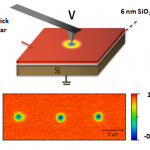
- Figure 1: The schematic of the prepared sample and KFM image of the written charge dots into a 5-nm-thick molecular layer on a 4-nm-thick oxide layer.

-
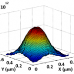
- Figure 2: Calculated stored charge density from the measured surface potential assuming uniform distribution of charge across the thickness of the trapping layer.

- P. Pavan, R. Bez, P. Olivo, and E. Zanoni, “Flash memory cells-An overview,” Proc. IEEE., vol. 85, no. 8, pp. 1248-1271,1997. [↩]
- International Technology Roadmap for Semiconductors, ITRS. (2007). [Online]. Available: http://www.itrs.net. [↩]
- P. K. Singh, R. Hofmann, K. K. Singh, N. Krishna, and S. Mahapatra “Performance and reliability of Au and Pt single-layer metal nanocrystal flash memory under NAND (FN/FN) operation,” IEEE Trans. Electron Devices, vol. 56, no. 9, Sep. 2009. [↩]
- S. Paydavosi, H. Abdu, G. J. Supran, V. Bulović, “Performance Comparison of Different Organic Molecular Floating Gate Memories,” IEEE Trans. Nanotechnology, vol. 10, no. 3, May 2011. [↩]