Power and Performance Optimized SRAM Caches for Exascale Processors
- Category: Circuits & Systems
- Tags: Anantha Chandrakasan, Yildiz Sinangil
On-chip memories are responsible for a large portion (40% by many estimates) of the total energy consumption and area of modern processor designs. Therefore, memory optimization for density, power, and frequency trade-offs is crucial to meet the aggressive power goals for the exascale processors. Today’s cache bit-cells in 65-nm CMOS consume 1 pJ per access at 1.0 V. Our goal is to reduce this amount by a factor of 18 to Angstrom Project’s target at 11-nm technology. This gives us a clear target of 50 fJ energy per operation (E/Op) per bit-cell at 11-nm.
We are designing the first version of Angstrom microprocessor’s L1-cache using 65-nm CMOS. To decrease E/Op from ~1 pJ to ~200 fF per bit-cell, we designed our L1-cache bit-cells to work down to 0.5 V. SRAM bit-cells suffer from decreased stability at low-voltages. In Figure 1, read and write margins of a bit-cell are simulated by 1000-point Monte Carlo analyses at 0.5 V, and negative values indicate failures. To combat margin problems, the work in [1] uses an 8-transistor (8T) bit-cell. This bit-cell’s read port is de-coupled from the storage nodes as it is given in Figure 1, so it is immune to read-upsets. The remaining 6 transistors can be sized to favor writes.
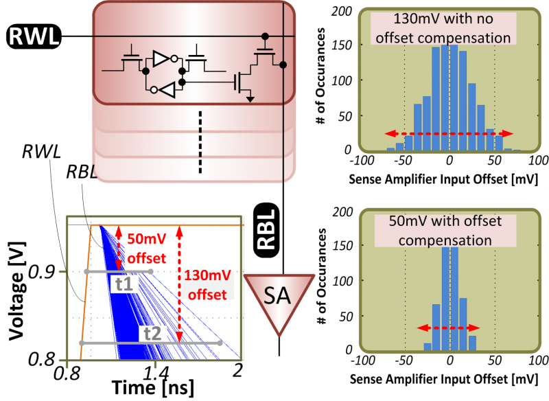
For the 8T bit-cell, a single ended sense amplifier (SA) is necessary since read-bit-line (RBL) is the only port used for the read operation. Different SA techniques have been analyzed such as non-strobed regenerative sensing [2] and strobed strong-arm based sensing; the latter is chosen due to its robust design and low-voltage compatibility. The offset of SA is reduced using offset-compensation techniques, and this concept is illustrated by 1000-point Monte Carlo analyses on input offset of our strong-arm type SA with or without compensation. All analyses shown are done on 22-nm predictive technology [3] .
-
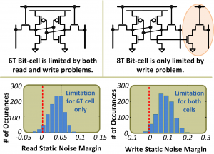
- Figure 1: The 8T bit-cell has two extra transistors compared to the 6T bit-cell. This way, its read port is isolated from its write port. Therefore, the 8T bit-cell has better static-noise-margin and can work at lower voltages.

-
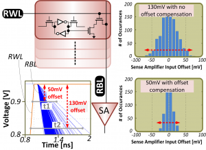
- Figure 2: Access time is limited by the worst-case bit-cell’s discharge time of the RBL by the worst case SA offset amount. Decreasing input offset from 130 mV to 50 mV results in almost 2 times less discharge time for the worst-case bit-cell.
- Chang, L.; Fried, D.M.; Hergenrother, J.; Sleight, J.W.; Dennard, R.H.; Montoye, R.K.; Sekaric, L.; McNab, S.J.; Topol, A.W.; Adams, C.D.; Guarini, K.W.; Haensch, W.; , “Stable SRAM cell design for the 32 nm node and beyond,” VLSI Technology, 2005. Digest of Technical Papers. 2005 Symposium on , pp. 128- 129, 14-16 June 2005. [↩]
- Verma, N.; Chandrakasan, A.P., “A High-Density 45nm SRAM Using Small-Signal Non-Strobed Regenerative Sensing,” Solid-State Circuits Conference, 2008. ISSCC 2008. Digest of Technical Papers. IEEE International, pp. 380-621, 3-7 Feb. 2008. [↩]
- N. Integration and T. Modeling (NIMO) Group, Arizona State Univ., “Predictive technology model,” 2008. [Online]. Available: http://ptm.asu.edu/. [↩]