Scaling of High Aspect Ratio Current Limiters for the Individual Ballasting of Large Arrays of Field Emitters
Field Emitter Arrays (FEAs) are excellent cold cathodes, but they have not found widespread adoption in demanding device applications because of several major challenges, including spatial/temporal current variations emanating from emitter tip radius distribution and the work function fluctuation. A consequence of tip radius variation is that the sharper emitters burn out from Joule heating before duller emitters turn on, reducing the current attainable from FEAs.
Addressing these challenges, groups have incorporated current limiting (ballasting) elements including large resistors [1] , diodes [2] , and MOSFETs [3] into FEAs, but none of these simultaneously provide high current, high emitter density, and high current density. Velasquez-Garcia et al. demonstrated silicon vertical ungated FETs integrated with FEAs, resulting in a Si tip on Si pillar structure [4] . The ungated FET has a current-source-like I-V characteristic, providing effective individual ballasting of emitters while allowing uniform and high current emission without thermal runaway [4] . To limit emission current, the device uses pinch-off and velocity saturation of carriers in a Si high aspect ratio channel. Their pillars have a diameter of 1 µm, height of 100 µm, and 10-µm pitch, resulting in a density of 106 emitters/cm2. However, a consequence of tip radius variation and ballasting is that the energy distribution of emitted electrons is larger when compared to un-ballasted FEAs.
To obtain FEAs with higher current densities, lower operating voltages, and reduced energy spread while retaining current uniformity, we expanded on previous work by scaling their tip on Si pillar structure. We developed vertical ungated FET current limiters 100 nm in diameter, 8 µm tall, and with 1-µm pitch, increasing the density to 108 emitters/cm2 (Figure 1). These devices demonstrate excellent current saturation of 15 pA / pillar with a linear conductance of 2.6×10⁻¹⁰ S/pillar and an output conductance under 10-13 S/pillar. The current saturates at a drain to source voltage under 0.2 V. These are the highest density, smallest diameter, and lowest operating voltage Si vertical ungated FETs ever reported.
-
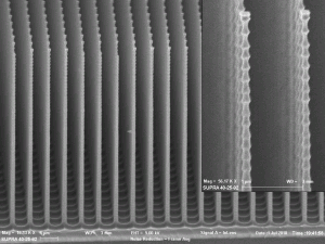
- Figure 1: Cross-sectional SEM of the vertical ungated FET structure with the passivation oxide removed. The pillars are 8 microns tall and taper to a diameter of 95 nm at the top.

-
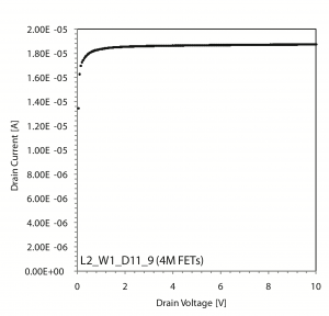
- Figure 2: Output characteristics of large arrays show good saturation at low VDS.

- P. Vaudaine and R. Meyer, “’Microtips’ fluorescent display,” IEDM Tech. Dig., 1991, pp. 197-200. [↩]
- Y. Kobori and M. Tanaka, “Field emission cathode,” U.S. Patent 5 162 704, Feb. 5, 1992. [↩]
- J. Itoh, T. Hirano, and S. Kanemaru, “Ultrastable emission from a metal–oxide–semiconductor field-effect transistor-structured Si emitter tip,” Applied Physics Letters, vol. 69, no. 11, pp. 1577–1578, 1996. [↩]
- L. F. Velasquez-Garcia, S. A. Guerrera, Y. Niu, and A. I. Akinwande, “Uniform high-current cathodes using massive arrays of Si field emitters individually controlled by vertical Si ungated FETs – Part 1: Device design and simulation & Part 2: Device fabrication and characterization.” IEEE Trans. Electron Devices, vol. 58, no. 6, pp. 1775-1791, June 2011. [↩] [↩]