The Effect of a Nitrogen Anneal on the Dark Current of Ge Photodiodes
- Category: Electronic Devices
- Tags: Judy Hoyt, Nicole DiLello
Germanium is a promising candidate for use in CMOS-compatible photodiodes. Its strong absorption in the 1.55-µm range and relative ease of integration on silicon substrates make it suitable for high-speed electronic photonic integrated circuits as well as in infrared sensors. To reduce power consumption and improve the signal-to-noise ratio, the diodes must have a low leakage current in reverse bias. This study has investigated the leakage current of germanium photodiodes grown by low-pressure chemical vapor deposition (LPCVD) using an Applied Materials epitaxial reactor. This study specifically looks at the effect of a post-metallization nitrogen anneal on the dark current.
To fabricate these diodes, germanium was grown epitaxially on a p+ Si substrate. The wafers then received an in-situ cyclic anneal to reduce the threading dislocation density. The wafers were subsequently implanted with phosphorus to create a vertical pin junction, passivated with a low temperature oxide, and contacted with metal. Following metallization, the wafers saw an optional anneal in nitrogen for 45 minutes at varying temperatures. Figure 1 shows the current v. voltage characteristics for a 10- x 10-μm square device at different temperatures. The dark current is reduced from 10 μA for diodes without an anneal to 8 nA for a sample with a 400°C anneal. To further investigate this effect, Ge-on-Si capacitors were made with LTO as their dielectric. They were annealed at the same temperatures as the diodes. Figure 2 shows the capacitance v. voltage measurements for different annealing temperatures. The anneal shifts the flatband voltage to the right, indicating that the anneal changes the fixed charge in the LTO. Without an anneal, the Ge surface is depleted, causing a high surface recombination velocity. After an anneal at 400°C, the surface is accumulated with holes, which reduces the recombination velocity and decreases the dark current.
-

- Figure 1: Dark current as a function of voltage for different annealing temperatures for a 10- x 10-μm device. The anneal reduces the dark current by ~1000X. The inset shows a cross-sectional schematic diagram of the Ge-on-Si photodiode.

-
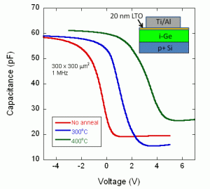
- Figure 2: Capacitance as a function of voltage for different annealing temperatures for a 300- x 300-μm device. The anneal shifts the curve to the right, increasing the flatband voltage. This shift implies a change in the fixed charge in the LTO, which changes the surface condition of the Ge. The inset shows a cross-sectional schematic diagram of the capacitor.
