Micro-contact Printed MEMS
- Category: MEMS & BioMEMS
- Tags: Apoorva Murarka, Jeffrey Lang, Vladimir Bulovic
It is desirable to extend the functionality of MEMS to different form factors including large area arrays of sensors and actuators, and to various substrate materials, by developing a means to fabricate large-area suspended thin films. Conventional photolithography-based MEMS fabrication methods limit the device array size and are incompatible with flexible polymeric substrates. We present a new method for fabricating thin (140-nm-thick) suspended metal films in MEMS using micro-contact printing. These films can be utilized in pressure sensors, microphones, deformable mirrors, tunable optical cavities, and large-area arrays of MEMS sensors.
Our approach to MEMS fabrication involves the use of a stamp and a donor viscoelastic transfer pad that is coated with an organic release layer and a thin film of metal. The stamp consists of a layer of patterned polydimethylsiloxane (PDMS) atop a glass slide that is coated with a layer of electrically conducting indium tin oxide (ITO). The surface of this patterned PDMS stamp is placed in contact with the thin metal film on the donor transfer pad, and then the stamp is rapidly peeled away, picking up the metal film. The metal film ends up bridging the gaps in the patterns of the PDMS stamp, forming a capacitive MEMS structure. A continuous film of metal is lifted onto the stamp only if the stamp is peeled off the transfer pad rapidly.
This process avoids the use of solvents and etchants, eliminating the need for deep reactive-ion etching and other harsh chemical treatments. Solvent absence during fabrication also avoids the detrimental effects of MEMS stiction that can result during wet processing. MEMS fabrication on flexible polymeric substrates is also possible due to the absence of elevated temperature processing.
Thin films up to 0.78 mm2 in area have been fabricated using the aforementioned process, as shown in Figure 1. These MEMS devices are actuated electrostatically to demonstrate the deflection of 25-μm-diameter films (see Figure 2).
-
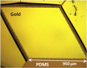
- Figure 1: An optical microscopy image of the pressure sensor fabricated using the contact lift-off mesa-transfer process. The gold parallelogram is the pressure sensor. About 1024 circular cavities are covered by this parallelogram gold membrane, which is 140 nm thick. The underlying PDMS on ITO-Glass is patterned with 25-µm- diameter circular cavities with about 5-µm to 7-µm spacing between the circles.

-
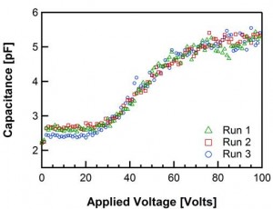
- Figure 2: Three capacitance-voltage sweeps for a single device. The increase in the capacitance of the device with voltage indirectly demonstrates deflection of the gold membrane, which bows under the electrostatic force to decrease the gap spacing over the air cavities in the PDMS spacer layer, thus increasing the capacitance.

- A. Murarka, C. Packard, F. Yaul, J. Lang, and V. Bulovic, “Micro-contact printed MEMS,” in 2011 IEEE 24th International Conference on Micro Electro Mechanical Systems (MEMS), pp. 292-295, 23-27 Jan. 2011.
- C. Packard, A. Murarka, E. W. Lam, M. A. Schmidt, and V. Bulovic, “Contact-printed microelectromechanical systems,” Advanced Materials, vol. 22, pp. 1840–1844, 2010.