Metal Oxide Transistors for Large Area Electronics
- Category: Circuits & Systems, Electronic Devices
- Tags: Akintunde Akinwande, Annie Wang, Charles Sodini, Vladimir Bulovic
Optically transparent, wide band gap metal oxide semiconductors are a promising candidate for large area flexible electronics. Because most commercially available flexible substrates, particularly polymer substrates, cannot withstand the high temperature processing (>400°C) required for traditional silicon device fabrication, the development of new materials and devices that can be processed at low temperatures in a scalable manner is needed. Metal oxide semiconductors have been demonstrated to retain high carrier mobilities even in the disordered, amorphous state obtained when processed at near-room temperatures [1] [2] . Compared to amorphous silicon field effect transistors (FETs), which are the dominant technology used in display backplanes, metal-oxide-based FETs have been demonstrated with higher charge carrier mobilities, higher current densities, and faster response performance [3] [4] .
It has been shown both in simulation and by experiment that FET threshold voltage (VT) can be modified simply by changing the channel layer thickness, without requiring the additional complexity of multiple channel materials or different dopings. In this project we have developed a low temperature (~100°C), scalable lithographic process for top-gate, bottom-contact amorphous metal oxide-based FETs using parylene, a room temperature-deposited CVD polymer, as gate dielectric. Figure 1 shows a micrograph of an array of FETs fabricated with different channel lengths. The baseline process was extended to enable the integration of FETs with different threshold voltages on the same substrate. The availability of FETs with different threshold voltages enables the implementation of enhancement/depletion (E/D) logic circuits that have faster speeds and smaller device areas than single-VT topologies. Using the two-VT lithographic process, we fabricated and characterized integrated E/D inverters and ring oscillators that operate rail-to-rail at supply voltages as low as VDD = 3V. An example inverter characteristic is plotted in Figure 2. These results demonstrate the potential for low VDD metal oxide-based integrated circuits fabricated in a low temperature budget, fully lithographic process for large area electronics.
-
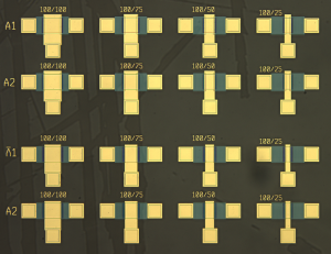
- Figure 1: An array of metal oxide FETs with varying channel lengths fabricated in a low-temperature-budget (~100°C) process. The lithographic process enables integration of these FETs into large-area electronic circuits.

-
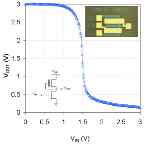
- Figure 2: DC inverter transfer characteristic for an enhancement/ depletion inverter fabricated using the two-VT metal oxide FET process. For both driver and load FETs, W/L = 100 μm/25 μm. At VDD = 3V, inverter gain is >20 and noise margins are >1V on either side.

- K. Nomura, H. Ohta, A. Takagi, T. Kamiya, M. Hirano, and H. Hosono, “Room-temperature fabrication of transparent flexible thin-film transistors using amorphous oxide semiconductors,” Nature, vol. 432, pp. 488-492, Nov. 2004. [↩]
- J. Robertson, “Disorder and instability processes in amorphous conducting oxides,” Physica Status Solidi B-Basic Solid State Physics, vol. 245, pp. 1026-1032, June 2008. [↩]
- R. L. Hoffman, B. J. Norris, and J. F. Wager, “ZnO-based transparent thin-film transistors,” Applied Physics Letters, vol. 82, pp. 733-735, Feb. 2003. [↩]
- E. Fortunato, P. Barquinha, G. Goncalves, L. Pereira, and R. Martins, “High mobility and low threshold voltage transparent thin film transistors based on amorphous indium zinc oxide semiconductors,” Solid-State Electronics, vol. 52, pp. 443-448, Mar. 2008. [↩]