Heterogeneous Integration of GaN and Si Devices
- Category: Electronic Devices
- Tags: Hyung-Seok Lee, Tomas Palacios
Gallium nitride (GaN) is a wide bandgap semiconductor with unsurpassed properties for high voltage switches and RF amplifiers. However, in spite of their excellent performance, GaN devices cannot compete with the integration density and complexity of modern Si CMOS electronics. The integration of GaN and Si (100) devices on the same chip would, therefore, enable a vast array of new applications, from novel power distribution schemes in Si microsystems, to power digital-to-analog converters and new opportunities for optoelectronic devices integrated on a Si platform.
Our GaN-Si integration approach is based on a full 4” wafer bonding [1] , where a thin layer of high-quality Si (100) is transferred to the top of a GaN-on-Si (111) wafer. These new hybrid wafers look akin to SOI wafers, except that instead of silicon underneath the oxide, there is a GaN device layer. Using this approach, PMOS devices and GaN HEMTs have been fabricated on the same wafer. Figure 1 (left) shows a cross-sectional view of the bonded 4” GaN and Si wafers. Once the hybrid wafer has been fabricated, a standard Si process technology was used for the fabrication of the Si devices. After the fabrication of the Si devices, windows are opened to expose the III-N epilayer in the regions where GaN HEMTs are required. Figure 1 (right) shows the optical microscope image of a fabricated a Si PMOS and a GaN HEMT devices in close proximity. Figure 2 (top) shows the typical output characteristics of a Si pMOSFET with gate length (Lg) of 3 µm and a GaN HEMT with Lg=3.2 µm. A GaN HMET shows a less than 5% difference with a reference HEMT, indicating that this integration process using hybrid wafers has not been influenced on the device characteristics due to the high thermal stability of the fabricated Si/GaN/Si wafers.
-
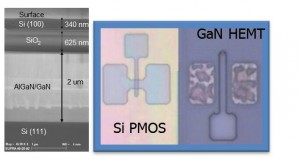
- Figure 1: Scanning electron microscope (SEM) image of the cross-sectional view of a Si-GaN-Si bonded wafer (left). Optical image of the fabricated Si PMOS and GaN HEMT on a 4-inch Si(100)-GaN-Si(111) hybrid wafer (right).

-
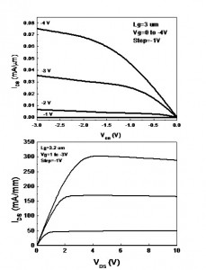
- Figure 2: DC output characteristics of a Si pMOSFET with Lg=3 µm (top) and GaN HEMTs with Lg=3.2 µm (bottom).

- K. Ryu, J. Chung, B. Lu, and T. Palacios, “Wafer bonding technology in nitride semiconductors for applications in energy and communications,” ECS Transactions, vol. 33, no. 4, pp. 125-135, 2010. [↩]