category » Materials
Due to its high band gap energy and superb electronic-carrier mobilities, GaN is fast becoming the material of choice for…
Semiconducting nanowire-based solar cells have gained interest because of their potential to achieve one-dimensional charge transport pathways and large interfacial…
Ge nanowires are of interest for future sub-10-nm gate length p-MOSFETs because of the excellent electrostatic control afforded by the…
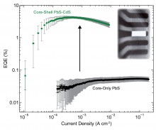
Here we demonstrate a solution-processed ordered bulk heterojunction quantum dot (QD) solar cell with AM1.5G power conversion efficiencies of up…

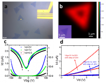
Monolayer MoS2, a transition metal dichalcogenide, is a novel flexible semiconducting material with a 1.8 eV direct band gap. Recent…
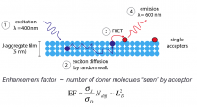
We show patterning of thin J-aggregate[1] films using nano-imprinting. Unlike the conventional microfabrication techniques, such as direct-write or lift-off processes,…
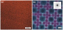
Colloidal semiconductor nanocrystals or quantum dots (QDs) offer size-tunable absorption and luminescence spectra, permitting a broad range of applications in…
Near-infrared light sources integrated at room temperature with any planar surface could be realized by harnessing the broad spectral tunability,…
GaN FETs offer superior advantages in high-voltage and high-temperature operation due to its large bandgap (3.4 eV) and high breakdown…
Nanostructured solar cells attract increasing attention as a promising photovoltaic (PV) technology[1]. Generation of free charge carriers in nanostructured PV…
After enabling much of the modern world for more than 60 years, in the near future electronics will develop in…
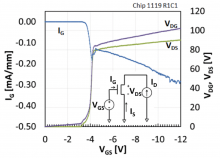
Achieving a sharp subthreshold swing (S) is crucial to enable the supply voltage scaling that is necessary to reducing power…
Currently bulk Bi and BixSb1-x have the best known thermoelectric (TE) properties at cryogenic temperatures. These properties can be further…
Transfer printing of thin metal films enables the fabrication of both planar and suspended membrane electrodes for microelectromechanical (MEMS) sensors…
Quantum dots (QDs) are exciting materials because their bandgap is dependent on the dot size. The use of QDs allows…
Detection of high-energy radiation (e.g., γ-rays) is key in nuclear non-proliferation strategies. When a wide-band gap semiconductor detector intercepts a…
Thermal management in nanoscale materials dramatically affects the efficiency of novel energy generation technologies, and engineering devices with appropriate heat…
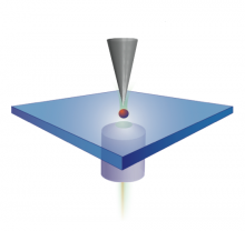
We report a technique for observing the dynamic behavior of a liquid contact line on superhydrophobic surfaces at high magnification…
Due to their mechanical, thermal, and electrical properties and their natural ability to grow on a variety of metallic and…
Small-molecule organic photovoltaic cells (OPVs) have the potential to be a low-cost, flexible power conversion solution to many energy problems[1]….
The diffusion of excitonic energy from within the photosensitive layer of a photovoltaic cell towards the charge separation interface is…
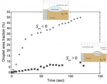
Despite years of advancement in making energy systems more efficient, the predominant mode of condensation seen in large-scale industrial processes…
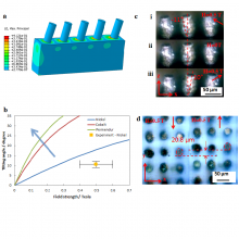
Water condensation on surfaces is a ubiquitous phase-change process that plays a crucial role in nature and across a range…
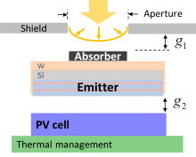
Solar thermophotovoltaic (STPV) devices have the potential to overcome the Shockley-Queisser limit by converting solar radiation to a narrow-band thermal…
Vapor condensation is observed in everyday life and routinely utilized in industry as an effective means of transferring heat. In…
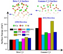
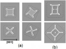
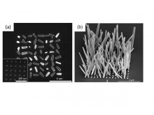
Portland cement clinker contains four major phases; alite (C3S) is the most dominant (50-70% by mass) and highly reactive with…
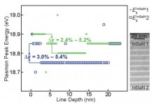
Solid state light-emitting diodes (LEDs) containing InxGa1-xN (0 ≤ x ≤ 1)/GaN hetrostructures as active components are of particular importance…
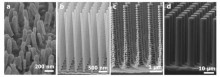
Nanowires combine the intrinsic properties of semiconductors with low dimensionality, which makes them potential building blocks for optoelectronic applications. GaAs…
Understanding the oxygen reduction reaction (ORR) kinetics at solid oxide fuel cell (SOFC) cathodes is considered critical for enhanced performance,…
Combustion of fossil fuels, essential for electricity generation and vehicular propulsion, is generally incomplete, leading to harmful NOx, CO, and…
Significant technological progress of organic semiconducting structures has led to their commercialization in the form of organic LED displays, solid…
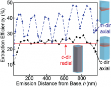
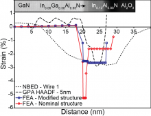
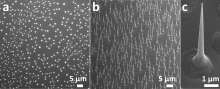
III-nitride nanowire-based light-emitting diodes (LEDs) are promising alternatives to thin-film LEDs for solid-state lighting[1]. Facile strain relaxation in nanowires allows…
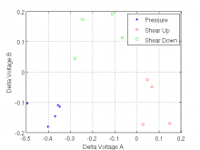
In the fields of robotics and prosthesis design, there is need for inexpensive, wide-area pressure- and shear-sensing arrays that can…
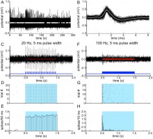
Probing and stimulating neural tissue is important to understand fundamentals of information processing and pathologies of the nervous system such…
The main goal of this work is to introduce functional natural materials into the design of surface plasmonic structures and…
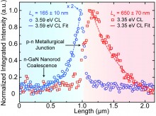
GaN-based nanowires and nanorods are promising materials systems for optoelectronic applications such as high efficiency light emitting diodes[1],[2] or low…
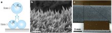
Micro- and nanostructured surfaces have broad applications ranging from liquid transport in microfluidics and cell manipulation in biological systems to…
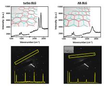
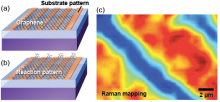
The growth of large-area bilayer graphene has been of technological importance for graphene electronics. The successful application of graphene bilayers…
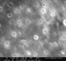
Thin films are generally metastable in the as-deposited state and will dewet (agglomerate) when heated. Nanometer scale films (<100 nm…
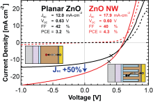
Photovoltaics (PVs) with inorganic zinc oxide nanowire (ZnO NW) active layers are possible for future generations of technology due to…
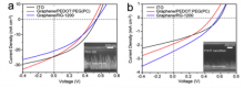
The successful fabrication of optoelectronics on economical, flexible, and lightweight substrates such as plastic and paper could pave the way…
Graphene has exceptional electronic, optical, mechanical, and thermal properties, which provide it with great potential for use in electronic, optoelectronic…
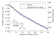
A co-crystal is a crystalline material made up of two or more components. In pharmaceutical systems, co-crystallization is frequently used…
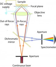
Nature presents us with a fundamental mismatch between the “size” of visible light (~250 nm in free space) and the…