Correlation of Doping, Structure and Carrier Dynamics in a Single GaN Nanorod
- Category: Materials, Nanotechnology, Optics & Photonics
- Tags: silvija gradecak, xiang zhou
GaN-based nanowires and nanorods are promising materials systems for optoelectronic applications such as high efficiency light emitting diodes[1],[2] or low lasing threshold lasers[3],[4]. To improve device design and fabrication based on these nanostructures, nanoscale correlation of heterostructure properties to doping and alloying are essential. We report nanoscale optical investigation of GaN p-n junction nanorods by cathodoluminescence (CL) in scanning transmission electron microscopy (STEM), a non-destructive and facile way to study doping and alloying with high spatial resolution, at both room and cryogenic temperatures. The GaN nanorods were grown by plasma-assisted molecular beam epitaxy (PAMBE) and doped with Si and Mg for respective n- and p-type doping. The position of the Mg acceptor level was identified at 0.24 eV above the valence band by comparing the CL spectra in n- and p-doped GaN in the same nanorod (Figure 1). Intensity profiles of CL emissions characteristic of dopant-related transitions were used to determine precisely the position of the p-n junction. CL quenching inside the nanorod was attributed to structural defects due to nanorod coalescence at the nanowire base and unpassivated surface states in n- and p-doped nanorod portions, respectively. Minority carrier diffusion lengths of 160 nm and 650 nm in Si- and Mg-doped GaN, respectively, were extracted (Figure 2). Temperature-dependent CL study also reveals activation energy of 19 meV for non-radiative recombination in Mg-doped GaN nanorods, which is likely due to surface states. The measured optical emission, dopant level, and estimated carrier diffusion lengths from this study focusing on GaN nanorods are consistent with previous thin film studies. The defect-induced CL quenching highlights the importance of controlling nanorod coalescence during MBE growths and surface passivation for nanostructures to further improve their device performances.
-
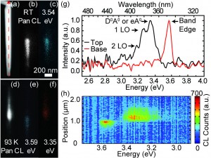
- Figure 1: (a) Dark-field STEM, (b) panchromatic, and (c) 3.54-eV monochromatic CL images of a single GaN p-n junction nanorod taken at RT. (d) Panchromatic, (e) 3.59-eV, and (f) 3.35-eV monochromatic CL images of the same nanorod at 93 K. (d) CL spectra of taken at top and base of the nanorod. (h) CL spectrum map along the length of the nanorod indicated by the dotted line in (a).
-
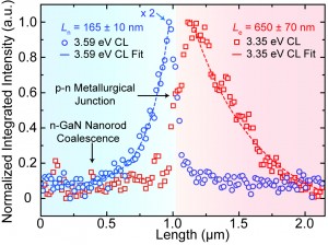
- Figure 2: Normalized integrated intensities of the 3.59-eV and 3.35- eV CL luminescence along the length of the nanorod shown in Figure 2(h). The positions of the nanorod coalescence in the n-GaN section and metallurgical junction are indicated. The squares and circles are experimental data and the dashed lines are fits based on an exponential decay model.
- Y. J. Lu, H. W. Lin, H. Y. Chen, Y. C. Yang, and S. Gwo, “Single InGaN nanodisk light emitting diodes as full-color subwavelength light sources,” Applied Physics Letters, vol. 98, pp. 233101:1-3, Jun 6 2011. [↩]
- F. Qian, S. Gradečak, Y. Li, C. Y. Wen, and C. M. Lieber, “Core/multishell nanowire heterostructures as multicolor, high-efficiency light-emitting diodes,” Nano Letters, vol. 5, pp. 2287-2291, Nov 2005. [↩]
- S. Gradečak, F. Qian, Y. Li, H. G. Park, and C. M. Lieber, “GaN nanowire lasers with low lasing thresholds,” Applied Physics Letters, vol. 87, pp. 173111:1-3, Oct 24 2005. [↩]
- Y. J. Lu, J. Kim, H. Y. Chen, C. H. Wu, N. Dabidian, C. E. Sanders, et al., “Plasmonic Nanolaser Using Epitaxially Grown Silver Film,” Science, vol. 337, pp. 450-453, Jul 27 2012. [↩]