Understanding the Light Emission Mechanisms in InGaN by Correlating its Structural and Optical Properties
- Category: Energy, Materials, Optics & Photonics
- Tags: kamal baloch, silvija gradecak
Solid state light-emitting diodes (LEDs) containing InxGa1-xN (0 ≤ x ≤ 1)/GaN hetrostructures as active components are of particular importance because of their ability to emit intense light in the entire visible spectrum. However, the cause of their high light-emission efficiency is a matter of debate. Scanning transmission electron microscopy (STEM) and low-loss electron energy loss spectroscopy (EELS) studies conducted at voltages ≥ 200 kV have attributed strong emission to the formation of “large-scale”1-3-nm In-rich clusters[1]. However, this finding was questioned in a high resolution transmission electron microscopy (HRTEM) study, which argued that observed spinodal decomposition was caused due to knock-on damage by the 200 kV electron beam[2].
To understand whether or not InGaN alloy in these hetrostructures undergoes spinodal decomposition, we employed atomically resolved aberration (CS)-corrected STEM at 120 kV to demonstrate that this voltage is below the knock-on displacement threshold for InGaN as no discernible electron-beam damage was observed after a continuous exposure for extended periods of time (see Figure 1). To verify whether small contrast variations in the InGaN quantum wells (QWs) seen in Figure 1 correspond to a variation in In composition, ∆x, we employed low-loss EELS at 120 kV. By scanning the electron beam in QWs, identified as InGaN 1 and InGaN 2 in Figure 2, the energy of the plasmon peak (Ep), which is characteristically composition-dependent, is measured with a spatial resolution of 0.3 nm; Ep is plotted in Figure 2. By measuring ∆x, for each of the QWs separately, we determined that the measured changes in plasmon energies correspond to compositional variation of 5.4% or less, which is too small to be attributed to the existence of large-scale In-rich clusters. The next step is to correlate these structural and electronic properties with the optical properties with sub-wavelength resolution by employing a custom cathodoluminescence set-up incorporated in a STEM.
-
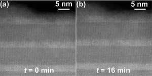
- Figure 1: Time-series of the three InGaN QWs separated by GaN barriers acquired by CS-STEM at 120 kV at (a) t = 0 min and (b) t = 16 min. These images confirm that there is no beam-induced damage at 120 kV.
-
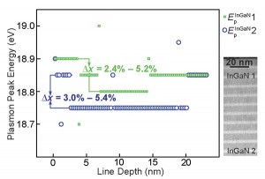
- Figure 2: Energy of the plasmon peak (Ep) extracted from low-loss EELS data plotted as a function of scan position. The compositional variation corresponding to the observed changes in Ep is < 5.4%, which suggests that there are no large-scale In-rich clusters present.
- J. R. Jinschek, R. Erni, N. F. Gardner, A. Y. Kim, and C. Kisielowski, “Local indium segregation and bang gap variations in high efficiency green light emitting InGaN/GaN diodes,” Solid State Communications, vol. 137, pp. 230-234, Jan 2006 [↩]
- T. M. Smeeton, M. J. Kappers, J. S. Barnard, M. E. Vickers, and C. J. Humphreys, “Electron-beam-induced strain within InGaN quantum wells: False indium “cluster” detection in the transmission electron microscope,” Applied Physics Letters, vol. 83, pp. 5419-5421, Dec. 29 2003. [↩]