Effect of Morphology in Quantum Dot Electronics
- Category: Electronic Devices, Energy, Materials, Nanotechnology
- Tags: mark weidman, william tisdale
Quantum dots (QDs) are exciting materials because their bandgap is dependent on the dot size. The use of QDs allows for precise control over the wavelengths of light that are emitted or absorbed in applications such as light-emitting diodes or photovoltaic devices. Producing efficient devices made from QD films requires controlling the rates of charge transport and exciton diffusion among the QDs. Charge transport occurs via tunneling between neighboring QDs, so the interparticle spacing is a critical parameter[1] while the rate of exciton diffusion is a function of the center-to-center distance between QDs. Therefore the morphology of a QD film strongly impacts its electronic properties[2]. Whether the goal is to increase or decrease charge transport/exciton diffusion, it is important to be able to quantify the interparticle spacing and center-to-center distances. Figure 1a shows a transmission electron microscopy (TEM) image of lead sulfide QDs. Automated analysis of TEM images allows for the determination of the mean diameter and standard deviation, which in this case is 6.3 ± 0.4 nm. The top inset is an ideal hexagonally close packed lattice, where the different colors indicate shells of dots at the same distance from the reference dot (shown in black). The distance between the centers of every dot is calculated to give the center-to-center distance distribution in Figure 1b. The colored vertical lines in Figure 1b correspond to the shells of the same color in the ideal hexagonally close packed lattice. The first peak at 9.6 ± 0.5 nm represents the average center-to-center distance of the first neighbors in the QD film. Thus the distance between neighboring dots is calculated to be 3.3 ± 0.6 nm. Using these techniques, it is possible to better understand QD electrical properties by correlating them with film morphology.
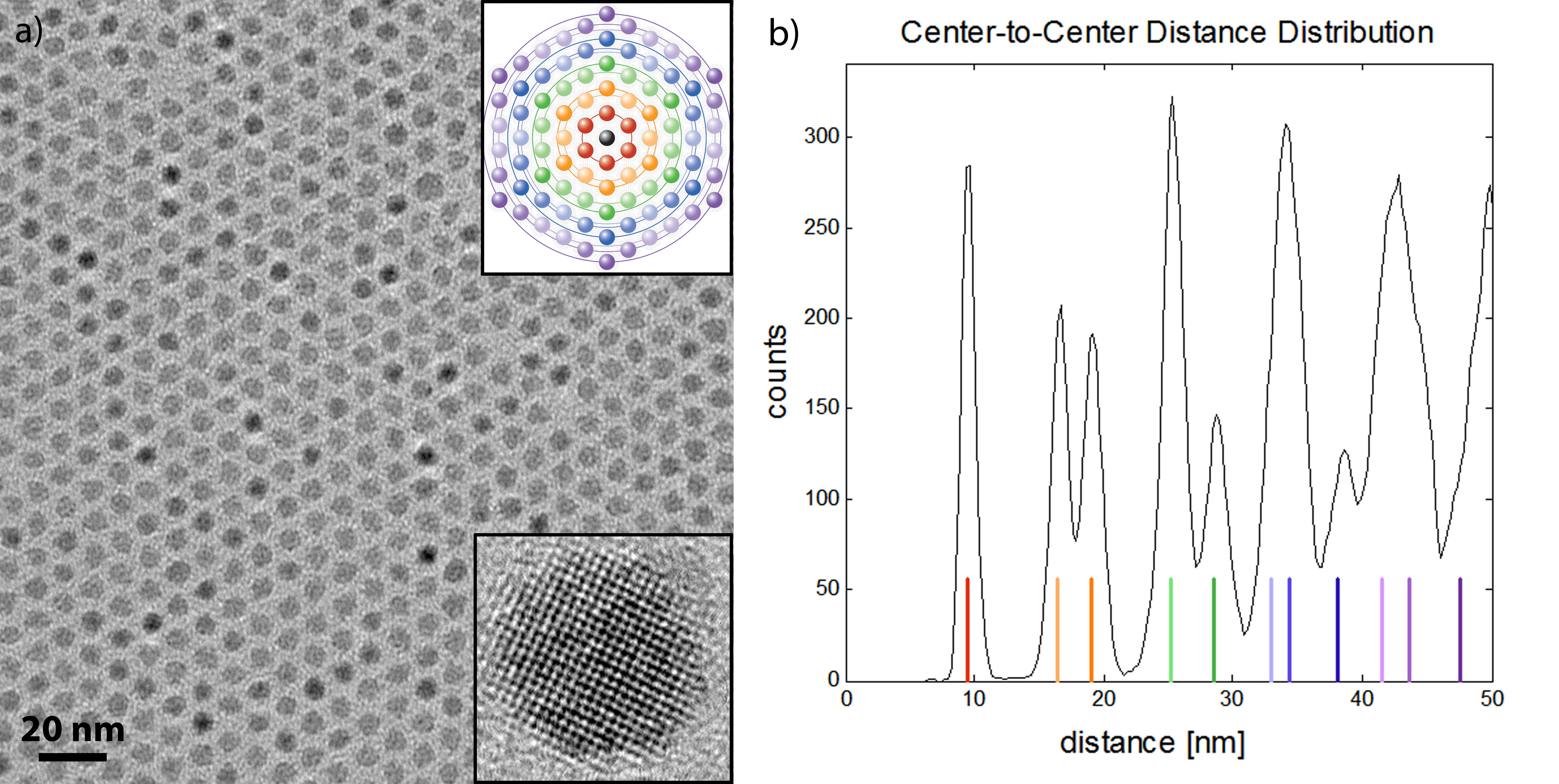
Figure 1: a) TEM image of highly monodisperse lead sulfide QDs capped with oleic acid ligands. The dots have a mean diameter of 6.3 nm (σ=6.0%) and show self-assembly into a hexagonal closely packed lattice system. An ideal hexagonally close packed lattice is shown in the top inset, with color used to indicate different shells of dots. The bottom inset is high-resolution TEM on a single QD to highlight its crystallinity. b) Center-to-center distance distribution of the main TEM image in Figure 1a, confirming the high degree of ordering in the film. The first major peak indicates an average center-to-center distance between nearest neighbors of 9.6 ± 0.5 nm.
- Y. Liu, M. Gibbs, J. Puthussery, S. Gaik, R. Ihly, H. W. Hillhouse, and M. Law, “Dependence of carrier mobility on nanocrystal size and ligand length in PbSe nanocrystal solids,” Nano Lett., vol. 10, pp. 1960-9, May 12 2010. [↩]
- D. V. Talapin, J.-S. Lee, M. V. Kovalenko, and E. V. Shevchenko, “Prospects of Colloidal Nanocrystals for Electronic and Optoelectronic Applications,” Chemical Reviews, vol. 110, pp. 389-458, 2010. [↩]