Nano-patterning of J-aggregate Thin Films
- Category: Energy, Materials, Nanotechnology, Optics & Photonics
- Tags: parag deotare, vladimir bulovic
We show patterning of thin J-aggregate[1] films using nano-imprinting. Unlike the conventional microfabrication techniques, such as direct-write or lift-off processes, which can be detrimental to polymers, we explore the possibility of using nano-imprinting technology for patterning thin film polymers. A 4.5 molecular layer of J-aggregate is grown using layer-by-layer deposition of thiacyanine dye coadsorbed over ployallylamine hydrocholoride (PAH) polyelectrolyte on a polydimethylsiloxane (PDMS) substrate. To allow for PAH’s poor adhesion with PDMS, the first PAH adsorption step was extended to 30 minutes to allow extra time for the initial adsorption via hydrophobic interactions[2]. This reduced adhesion property also helped in the pattern transfer. A master stamp consisting of nano-pillars is fabricated using ebeam lithography on SU8 resist spun on a silicon substrate. A 100-nm oxide layer is sputtered on the stamp to increase the adhesion between the j-aggregate film and the stamp. The stamp is then pressed gently on the j-aggregate thin film for about 10 s. Fluorescence microscope imaging is used to confirm the transfer process. Figure 1 shows the bright-field image of the patterned stamp used for the stamping process while Figure 2 shows the fluorescence image of the same area after pattern transfer. The results confirm a clean transfer of j-aggregate films onto the tip of the pillars. This successful high-yield, large-area patterning process not only opens new possibilities of designing devices in polymer thin films but also allows us to study and control excitons in such materials.
-
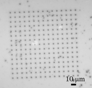
- Figure 1: Brightfield image showing the patterned structure on a silicon substrate. The patterns were defined using ebeam lithography on SU8 resist followed by sputtering of 100 nm of silicon dioxide.
-
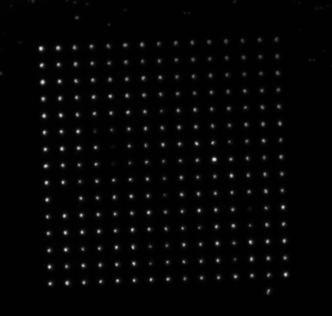
- Figure 2: Fluorescence image of the area shown in Figure 1. The results confirm the high yield of the transfer process.