Electronics on MoS2 and Other 2D Semiconductors
- Category: Electronic Devices, Materials, Nanotechnology
- Tags: lili yu, tomas palacios
After enabling much of the modern world for more than 60 years, in the near future electronics will develop in new dimensions with diverse functionalities. Ubiquitous electronics, represented by flexible displays, intelligent clothing, smart health diagnostics, autonomous homes, and wearable computing, will be a very important component of future electronics[1],[2]. The novel 2D material family based on layered transition metal dichalcogenides (MX2, M=Mo, W, X=S, Se, Te) offers great advantages for ubiquitous electronics. These materials are only a single molecular layer thick. They are mechanically flexible and optically transparent. They also have excellent thermal conductivity, high mobility, and a variety of energy band gaps.
In the past years, we have investigated the transport properties of different single-layer transition metal dichalcogenides: MoS2, MoSe2, WS2, and WSe2 synthesized by chemical vapor deposition[3],[4]. As an example, the transistors on single-layer WSe2 show ambipolar properties where both electrons and holes can be introduced by tuning the gate voltage (Figure 1). We further performed wafer-scale fabrication of top-gated DC and RF transistors and fully integrated digital and analog circuits on large scale single-layer MoS2, as shown in Figures 2 a, b, and c[5],[6]. The MoS2 devices show n-type properties with on-state current as high as 16 uA/um with on/off current ratio exceeding 108, giving the device great potential for ultra-low-power applications. RF devices with LG=300 nm show an fT of 900 MHz, an fmax of 1 GHz and a peak transconductance of ~3 uS/um. We have also fabricated logic inverters that operate under a wide range of Vdd, from 0.5 V to 5 V, with a peak voltage gain of ~20 at Vdd=5 V. A 1-bit analog-to-digital converter (ADC) is constructed (Figure 2a) based on a matched long-tail pair differential amplifier (Figure 2b). The ADC successfully converts a 1-kHz sinusoidal signal to a square wave, demonstrating the capability of MoS2 for both digital and analog application.
-
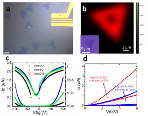
- Figure 1: (a) Optical image of CVD-grown WSe2 flakes directly grown on SiO2/Si substrate and the back-gated devices on the flake. The triangular shape is consistent with the lattice crystal structure of WSe2 and indicates the high quality of the synthesized sample. (b) Photoluminescence signal mapping of WSe2 flakes. The darker triangle in the center demonstrates thicker islands. (c) Transfer properties of CVD WSe2 back gate devices in linear scale (left) and similog scale (right). Electrons conduct at the high positive back gate voltage region, and holes conduct at the negative bias region. (d) Output performance of WSe2 FET with different back gate bias.
-
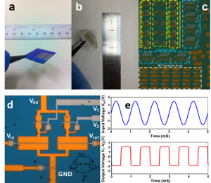
- Figure 2: Transistors and integrated circuits fabricated at the wafer scale using single-layer MoS2 grown directly on (a) a SiO2/Si substrate and (b) a sapphire substrate by CVD methods. (c) Optical micrograph of the fabricated chip showing arrays of RF transistors, currents sources, and 1-bit and 2-bit analog-to-digital converters (ADC). (d) Optical micrograph of a fully integrated 1-bit ADC constructed on single-layer MoS2. (e) Schematic circuit for the ADC. (c) AC coupled oscilloscope readings of the input and output signals (1kHz) of the ADC. The ADC is essentially a voltage comparator based on a differential amplifier with a matched long-tail pair configuration, which requires well-matched characteristics in the transistors involved.
- A. Nathan, et al., “Flexible electronics: The next ubiquitous platform,” in Proceedings of IEEE, vol. 100, pp. 1486-1517, 2012. [↩]
- S. R. Forrest, et al., “The path to ubiquitous and low-cost organic electronic appliances on plastic,” Nature, vol. 428, pp. 911–918, 2004. [↩]
- Y.-H. Lee et. al., “Synthesis of Large-Area MoS2 Atomic Layers with Chemical Vapor Deposition,” Adv. Mater., vol. 24, no. 17, pp. 2320-2325, 2012. [↩]
- Y.-H. Lee, L. Yu, et al., “Synthesis and Transfer of Single Layer Transition Metal Disulfides on Diverse Surfaces,” Nano Lett., vol. 13 (4), pp. 1852–1857, 2013. [↩]
- H. Wang, L. Yu et al., “Integrated Circuits Based on Bilayer MoS2 Transistors,” Nano Lett., vol. 12, no. 9, pp. 4674-4680, 2012. [↩]
- H. Wang, L. Yu et al., “Large-scale 2D Electronics based on Single-layer MoS2 Grown by Chemical Vapor Deposition,” arXiv preprint arXiv:1302.4027, 2012. [↩]