Self-assisted GaAs Nanowire Growth by MOCVD
- Category: Energy, Materials, Nanotechnology
- Tags: sema ermez, silvija gradecak
Nanowires combine the intrinsic properties of semiconductors with low dimensionality, which makes them potential building blocks for optoelectronic applications. GaAs nanowires are of particular interest for solar cell applications due to the high absorption coefficient and high electron mobility of GaAs. Common bottom-up nanowire growth methods involve metal seed particles to achieve one-dimensional growth; however, metal seeds can introduce impurities into nanowires that can deteriorate their optoelectronic properties[1]. Self-assisted growth mechanism, in which one of elements of nanowire is used as a seed particle, eliminates possible contamination from the seed particles. Self-assisted GaAs nanowires grown via molecular beam epitaxy have been reported in the literature[2], but metal-organic chemical vapor deposition (MOCVD) has not been explored so far despite the fact that MOCVD is an industrial-scale technique that can yield high growth rates and high nanowire throughput.
In this study, we have grown GaAs nanowire arrays using in-situ deposited Ga droplets as seed particles. Nanowire growth is realized by a two-step approach in MOCVD: high-temperature in-situ Ga droplet formation followed by low-temperature nanowire growth using Ga droplets as seed particles. The two-step approach has been found crucial; high temperatures are required for efficient Ga precursor decomposition and large surface diffusion length of Ga adatoms, which affect the nanowire density and diameter. On the other hand, lower growth temperatures are necessary to promote one-dimensional growth and to minimize lateral growth on nanowire facets. Nanowire density is around 8×10⁶ nanowires/cm2 as determined from top-view SEM images, such as Figure 1a. Figure 1b shows the nanowire array tilted at 45°, with average nanowire length around 4.6 μm. Nanowires have a tapered geometry due to Ga droplet consumption during growth (Figure 1c). By utilizing in-situ deposited Ga droplets as seed particles, we have achieved contamination-free GaAs nanowire arrays suitable for optoelectronic applications.
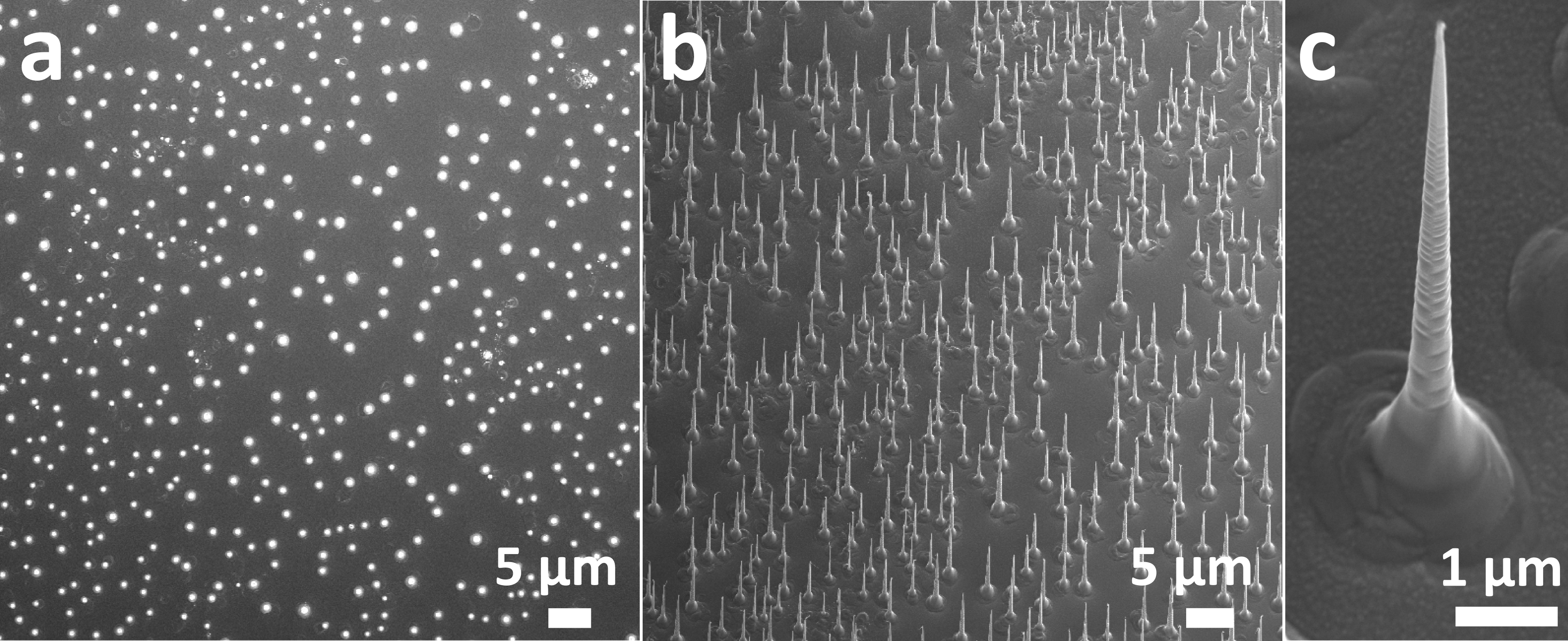
Figure 1: (a) Top-view SEM image of GaAs nanowire array showing nanowire density and uniformity. (b) 45° tilted nanowire array reveals average height of nanowires as 4.6 μm. (c) Nanowires have a tapered morphology due to consumption of Ga seed particle.
- M. J. Tambe, S. Ren, and S. Gradečak, “Effects of Gold Diffusion on n-Type Doping of GaAs Nanowires,” Nano Lett. vol. 10, no. 11, pp. 4584–4589, Nov. 2010. [↩]
- C. Colombo, D. Spirkoska, M. Frimmer, G. Abstreiter, and A. Fontcuberta i Morral, “Ga-assisted catalyst-free growth mechanism of GaAs nanowires by molecular beam epitaxy,” Phys. Rev. B, vol. 77, no. 15, p. 155326, Apr. 2008. [↩]