Lithographically-defined ZnO Nanowire Growth
- Category: Materials, Nanotechnology
- Tags: karl berggren, samuel nicaise
Photovoltaics (PVs) with inorganic zinc oxide nanowire (ZnO NW) active layers are possible for future generations of technology due to low-temperature processing, abundant materials, and application on many surfaces. For maximum performance, vertical alignment, density, and electrical properties of the NW, growth must be controlled. NWs with varying sizes, orientations, and pitch can be grown via a low-temperature, hydrothermal, seeded growth process with a zinc nitrate hexahydrate and hexamethylenetetramine solution[1]. To achieve an ideal NW spacing for PVs[2], growth spacing can be controlled with poly(methyl methacrylate) (PMMA) or block copolymers (BCPs) pre-patterned masks. We grew arrays of ZnO NWs that were masked by both poly(styrene-b-dimethylsiloxane) (PS-b-PDMS) BCP and PMMA hole arrays.
For a BCP nanopattern mask, a thin film of PS-b-PDMS was self-assembled on a ZnO seed-layer to form a single layer of oxidized, parallel PDMS cylinders (pitch = 35 nm) (Figure 1a). The BCP mask controlled the density of NWs during the subsequent hydrothermal growth process to about 4.5×10¹⁰ unmasked vs. 2.4×10¹⁰ NWs/cm2 masked (Figure 1b and 1c). The BCP mask can be further directed by electron-beam lithography-based template (EBL)[3][4]. For a PMMA resist mask, arrays of EBL-defined holes were patterned in 50-200 nm thick PMMA on a ZnO seed-layer (Figure 2a inset). The ZnO NWs grew only through the templating holes (Figure 2a and b). A hydrothermal-solution concentration of 2 mM and 0.2 mM poly(ethyleneimine) (PEI) and hole pitch of 275 nm resulted in primarily orthogonal, roughly 125-200 nm diameter NWs. This work expands on previous experimental work by others, though we report masks of smaller (275-nm) pitch, on a spin-coated seed layer[5].
-
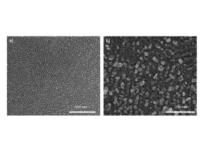
- Figure 1: Scanning-Electron Micrographs (SEM) of BCP and ZnO NWs grown through a BCP mask. a) Single layer of oxidized-PDMS cylinders from 45 kg/mol PS-b-PDMS BCP on a ZnO seed layer. b) and c) top-down and angled views of the nucleation of ZnO NWs. The nucleation points (therefore NW growth) are restricted to between the BCP cylinders.
-
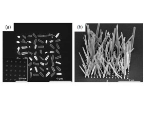
- Figure 2: Scanning-Electron Micrographs of ZnO NWs grown through EBL-defined PMMA masks with a 1-µm pitch. a) The growth of the NWs was not perpendicular to the substrate. (inset) PMMA hole mask before NW growth. b) The growth of the NWs was more perpendicular to the surface than in a) with a reduction of growth-solution molarity and addition of PEI.
- L. E. Greene, M. Law, D. H. Tan, M. Montano, J. Goldberger, G. Somorjai, and P. Yang, “General Route to Vertical ZnO Nanowire Arrays Using Textured ZnO Seeds,” Nano Lett., vol. 5, no. 7, pp. 1231-1236, (2005). [↩]
- I. J. Kramer, D. Zhitomirsky, J. D. Bass, P. M. Rice, T. Topuria, L. Krupp, S. M. Thon, A. H. Ip, R. Debnath, H.-C. Kim, and E. H. Sargent, “Ordered Nanopillar Structured Electrodes for Depleted Bulk Heterojunction Colloidal Quantum Dot Solar Cells,” Adv. Mat., vol. 24, no. 17, pp. 2315-2319, 2012. [↩]
- J. K. W. Yang, Y. S. Jung, J.-B. Chang, R. A. Mickiewicz, A. Alexander-Katz, C. A. Ross, and K. K. Berggren, “Complex self-assembled patterns using sparse commensurate templates with locally varying motifs,” Nat. Nanotech., vol. 5, pp. 256-260, 2010. [↩]
- A. Tavakkoli K. G., S. M. Nicaise, A. F. Hannon, K. W. Gotrik, A. Alexander-Katz, C. A. Ross, and K. K. Berggren, “Sacrificial-Post Templating Method for Block Copolymer Self-Assembly,” in review. [↩]
- S. Xu, Y. Wei, M. Kirkham, J. Liu, W. Mai, D. Davidovic, R. L. Snyder, and Z. L. Wang, “Patterned Growth of Vertically Aligned ZnO Nanowire Arrays on Inorganic Substrates at Low Temperature without Catalyst,” J. Amer. Chem. Soc., vol. 130, no. 45, pp. 14958-14959, 2008. [↩]