Nanoscale Stress State Characterization of InAlN/GaN Nanoribbon HEMT Structures
- Category: Electronic Devices, Materials, Nanotechnology
- Tags: eric jones, silvija gradecak
Due to its high band gap energy and superb electronic-carrier mobilities, GaN is fast becoming the material of choice for fabricating advanced optical and high-power electronic devices. Nanoribbon-structured high-electron-mobility transistor (HEMT) structures present a novel route towards strain engineering in GaN-based systems, which could lead to enhanced device performance[1]. In order to optimize the strain in these devices, however, it is important to quantify the strain in individual nanostructures. This work uses geometric phase analysis (GPA) and nanobeam electron diffraction (NBED) to quantify and map the strain over individual nanoribbon cross-sections, with nanometer resolution providing new insights into device evolution during fabrication inaccessible by other characterization techniques.
Nanoribbon structures were defined between the source and drain of planar HEMT structures using electron-beam lithography and dry-etching techniques. Lattice resolved images of individual ribbons were acquired using high-angular annular dark field (HAADF) and bright field (BF) scanning TEM (STEM) for GPA while line scans of NBED patterns were obtained from three different structures. Strain profiles were also simulated using a previously developed finite element analysis (FEA) model[2] for comparison to the experimental profiles.
Figure 1 shows a BF STEM image of a typical ribbon structure studied in this work with corresponding growth direction strain map. From this map a growth direction strain of -2.7% ± 0.5% with respect to the GaN substrate is measured in the HEMT layers. These measurements are confirmed by the NBED strain profiles, which also measure a strain of -2.7% ± 0.1% but with a precision five times greater than GPA. The experimental results suggest that the nominal compositions of the HEMT layers (see Figure 1) are not accurate. Use of linear elastic theory and energy dispersive X-ray spectroscopy enables calculation of the actual composition of each HEMT layer, which significantly improves strain profiles predicted by FEA as seen in Figure 2.
-
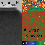
- igure 1: BF STEM image of a typical nanoribbon-structured HEMT studied in this work with layers labeled with nominal compositions. GPA is used to generate a map of the strain over the whole structure, clearly showing the strained HEMT layer.
-
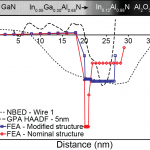
- Figure 2: Comparison of experimental and simulated strain profiles obtained from GPA, NBED, and FEA. The two simulated strain profiles demonstrate how the revised chemistries seen in the inset improved the FEA model.
- J. Kuzmik, A. Kostopoulos, G. Konstantinidis, J. F. Carlin, A. Georgakilas, and D. Pogany, “InAIN/GaN HEMTs: A first insight into technological optimization,” IEEE Transactions on Electron Devices, vol. 53, pp. 422-426, Mar 2006. [↩]
- E. J. Jones, M. Azize, M. J. Smith, T. Palacios, and S. Gradecak, “Correlating stress generation and sheet resistance in InAlN/GaN nanoribbon high electron mobility transistors,” Applied Physics Letters, vol. 101, 113101, Sep 2012. [↩]