Breakdown Voltage of High-voltage GaN FETs
- Category: Electronic Devices, Materials
- Tags: alex guo, jesus del alamo
GaN FETs offer superior advantages in high-voltage and high-temperature operation due to its large bandgap (3.4 eV) and high breakdown field strength (3.3 MV/cm). This combination of the large bandgap and high breakdown field makes these devices very attractive for power switching applications. In this regard, a key figure of merit is the breakdown voltage of the transistor, which must be high enough and stable. Most studies so far measure the breakdown voltage by driving the device to destruction, which does not allow a comprehensive study of the physics of breakdown. Our goal is to develop a benign off-state breakdown (BVOFF) measurement scheme so that reproducible, non-destructive breakdown measurements can be obtained. These measurements will allow us to understand the physics of breakdown and suggest approaches towards the engineering of breakdown voltage of GaN FETs.
To achieve non-destructive characterizations of the off-state breakdown voltage, BVOFF, we use the drain current injection technique proposed by our group[1]. We inject a constant drain current (of order 1 mA/mm) while ramping the gate from above threshold to below threshold. In this way, the device is driven to breakdown by simply turning it off. During the experiment, the gate current (IG), gate to drain voltage (VDG) and gate to source voltage (VDS) are recorded. Since the drain current is fixed, the device is not damaged during the measurement. Figure 1 shows an example of such measurement in a short-gate length GaN HEMT. As the device is turned off, VDS and VDG increase prominently, and a fraction of the current is diverted towards the gate. The fact that this transfer is not complete suggests that breakdown is limited by a channel mechanism such as punchthrough or impact ionization. In devices with gate lengths of 2.5 um or above, we have observed drain to gate breakdown as the injected drain current completely went through the gate when the device was turned off. During our measurements, we have found that severe trapping occurs. This limits their repeatability. We can successfully mitigate the trapping limitation through a high temperature bake (200°C for 10 minutes) performed after each measurement. This treatment yields reproducible measurements of the breakdown voltage. Systematic characterization of the breakdown voltage has allowed us to study the geometrical dependence of BVOFF on gate length and gate-to-drain spacing, as shown in Figure 2.
Next, we will study the temperature dependence of breakdown voltage in GaN HEMTs, in our effort to understand the physics of BVOFF. We will also study how the breakdown mechanism changes with device geometry and current level and investigate the role of trapping in the breakdown voltage measurements.
-
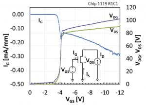
- Figure 1: Breakdown voltage measurement using the drain current injection technique (ID = 1 mA/mm). The inset shows the circuit diagram of this technique. As the device is turned off, we observe the onset of channel breakdown before gate breakdown. This phenomenon is typical for short-channel devices.
-
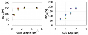
- Figure 2: Drain to source off-state breakdown voltage (BVDS) as a function of gate length and gate to drain gap. BVDS increases with LG and saturate at long LG. BVDS also increases with the gate to drain gap length.
- S. R. Bahl and J. A. del Alamo, “A new drain-current injection technique for the measurement of off-state breakdown voltage in FETs,” Electron Devices, IEEE Transactions on, vol. 40, no. 8, pp. 1558,1560, Aug. 1993. [↩]