Flexible High-Density MoS2 Sensor Arrays for Monitoring Action Potentials
- Category: Circuits & Systems, Energy, Materials, Medical Electronics
- Tags: charles mackin, tomas palacios
Monolayer MoS2, a transition metal dichalcogenide, is a novel flexible semiconducting material with a 1.8 eV direct band gap. Recent research has brought about flexible MoS2 transistors; highly sensitive NO gas sensors; and a number of MoS2 circuits including logic gates, SRAM cells, and oscillators[1][2][3][4]. Furthermore, a newly-developed MoS2 chemical vapor deposition (CVD) growth process now opens the doors to large-scale and cheap manufacture of monolayer films[5].
We are working on the use of CVD-grown MoS2 in biological and chemical sensors focusing on the specific application of implantable high-density and flexible sensor arrays for recording action potentials in sub-surface brain structures. Current state-of-the-art in vivo neuronal sensing is limited either to monitoring surface regions or to implanting rigid probes for sensing sub-surface regions of the brain[6]. Surface brain structures represent only a minute area of interest whereas rigid probes for sub-surface monitoring repeatedly slice brain tissue in response to micromovements. This action results in considerable tissue damage and scarring, which ultimately leads to poor neuronal contact and degraded signal detection. By incorporating both flexible MoS2 sensors and transistors into specialized probes for monitoring sub-surface structures, we plan to overcome some of the limitations in state-of-the art systems while providing further insights into the electronic and sensing capabilities of MoS2.
-
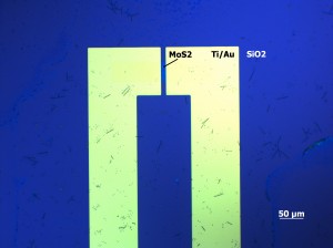
- Figure 1: Electrical double-layer transistor (EDLT) implemented using monolayer MoS2. MoS2 can be grown on a variety of substrates through chemical vapor deposition using S8 and MoO3 at 650°C. MoS2 channel regions are isolated via oxygen plasma etch. Ti/Au source-drain contacts are subsequently deposited using electron beam evaporation.
-
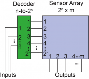
- Figure 2: MoS2 sensor array system architecture. Memory-inspired design employs encoded inputs to provide access to 2n sensor rows using n inputs. This configuration makes addressing and data extraction manageable for large sensors arrays.
- J. Pu, Y. Yomogida, K.-K. Liu, L.-J. Li, Y. Iwasa, and T. Takenobu, “Highly flexible MoS2 thin-film transistors with ion gel dielectrics,” Nano Letters, vol. 12, no. 8, pp. 4013–17, Aug. 2012. [↩]
- B. Radisavljevic, A. Radenovic, J. Brivio, V. Giacometti, and A. Kis, “Single-layer MoS2 transistors,” Nature Nanotechnology, vol. 6, no. 3, pp. 147–50, Mar. 2011. [↩]
- H. Li, Z. Yin, Q. He, H. Li, X. Huang, G. Lu, D. W. H. Fam, A. I. Y. Tok, Q. Zhang, and H. Zhang, “Fabrication of single- and multilayer MoS2 film-based field-effect transistors for sensing NO at room temperature,” Small, vol. 8, no. 1, pp. 63–67, Jan. 2012. [↩]
- H. Wang, L. Yu, Y.-H. Lee, Y. Shi, A. Hsu, M. L. Chin, L.-J. Li, M. Dubey, J. Kong, and T. Palacios, “Integrated circuits based on bilayer MoS₂ transistors,” Nano Letters, vol. 12, no. 9, pp. 4674–80, Sep. 2012. [↩]
- Y.-H. Lee, X.-Q. Zhang, W. Zhang, M.-T. Chang, C.-T. Lin, K.-D. Chang, Y.-C. Yu, J. T.-W. Wang, C.-S. Chang, L.-J. Li, and T.-W. Lin, “Synthesis of large-area MoS2 atomic layers with chemical vapor deposition,” Advanced Materials, vol. 24, no. 17, pp. 2320–25, May 2012. [↩]
- J. Viventi, D.-H. Kim, L. Vigeland, E. S. Frechette, J. a Blanco, Y.-S. Kim, A. E. Avrin, V. R. Tiruvadi, S.-W. Hwang, A. C. Vanleer, D. F. Wulsin, K. Davis, C. E. Gelber, L. Palmer, J. Van der Spiegel, J. Wu, J. Xiao, Y. Huang, D. Contreras, J. A. Rogers, and B. Litt, “Flexible, foldable, actively multiplexed, high-density electrode array for mapping brain activity in vivo,” Nature Neuroscience, vol. 14, no. 12, pp. 1599–605, Dec. 2011. [↩]