Tunable Surface Plasmonics on Electric-gated Nanostructures and its Coupling with Quantum Dot Emission
- Category: Materials, Nanotechnology, Optics & Photonics
- Tags: dafei jin, xuanlai fang
The main goal of this work is to introduce functional natural materials into the design of surface plasmonic structures and achieve largely tunable plasmonic behaviors, paving the way for future optical communication and information processing. Taking advantage of the evanescent coupling between emitted photons from a quantum dot and the excited surface plasmons at the material interface, we want to realize controllable quantum dot emission as well. Figure 1 shows a basic structure of our sample. A quartz crystal is used as the substrate, transparent to the incoming visible light. A silicon nanostructure about 40 nm high is patterned onto the substrate via electron beam lithography; this nanostructure serves both as a diffraction grating (or scatter), and as a grounding layer in this MOSFET-like construction. A 100-nm PMMA dielectric layer containing quantum dots of known concentration is spin-coated onto the nanostructure. The PMMA smoothes out the surface and provides a necessary insulating barrier for electric gating. A transparent conducting thin film, such as indium-tin oxide (ITO), and/or a ferroelectric thin film, such as barium titanate (BTO), of about 20 nm thick is sputtered on top of the PMMA. Then a gold film about 40 nm thick is sputtered on top; it works as an electrode for applying the gate voltage and also provides the electron source for surface plasmons, spanning the ITO/BTO and PMMA layers. A sufficiently large gate voltage can induce a high-density charge accumulation layer (for ITO) or surface charge termination (for BTO) at the vicinity of the PMMA and the thin film interface, which effectively drives a “phase transition” of the materials that changes the characteristic surface plasmon frequency in the spectrum. The coupling channel between the quantum dots and the surface plasmons can hence be effectively switched on and off, causing different lifetimes and emission rates. In experiments, we employ a standard confocal microscopy setup, as shown in Figure 2. The sample is illuminated by a continuous laser that covers the whole visible frequency range. The change of quantum dot emission spectrum is detected and recorded by a spectrometer.
-
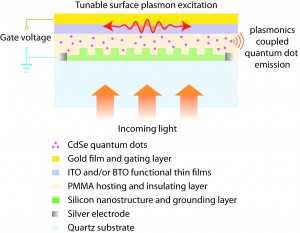
- Figure 1: Sample design for tunable surface plasmons and plasmonics-coupled quantum dot emission under electric gating.
-
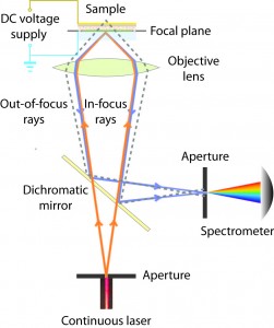
- Figure 2: Confocal microscopic setup for quantum dot emission measurement.