Applications of Nanoimprinted Structures In Organic Photovoltaics
- Category: Energy, Materials, Nanotechnology
- Tags: eletha flores, vladimir bulovic
Small-molecule organic photovoltaic cells (OPVs) have the potential to be a low-cost, flexible power conversion solution to many energy problems[1]. These OPVs take advantage of an extremely thin active layer, which enables this flexibility and reduces material volume. However, it is this thin quality that calls for improved power conversion efficiency compared to traditional silicon solar cells. Thin films suffer from reduced optical path lengths, which hinder light absorption and hence, power conversion efficiency. Many designs have been proposed to improve light absorption[2][3][4][5][6]. We present a novel light-trapping substrate geometry for OPVs that is based on a conformally coated, subwavelength-textured substrate design, which is intended to substantially increase optical path lengths. The subwavelength nature of these nanocones/nanowedges decouples the light propagation from the exciton diffusion path. This decoupling is an optimized situation for efficient charge transfer. Enhanced power absorption into the OPV active layer has been demonstrated via numerical computation methods, including COMSOL FEM (shown in Figure 1) and Lumerical FDTD. We will address the challenge to fabricate a working device by using nanoimprinting to create the structures in a conductive polymer, in which the nanoimprinting process is optimized to maintain good electrical properties of the patterned conductive film. We will also present an alternative approach that utilizes a conformal coating of the organic conductor PEDOT on the pre-patterned nanostructures, as shown in Figure 2. Uniform and conformal PEDOT coverage over the nanoscale features was achieved using an all-dry deposition process[7].
-
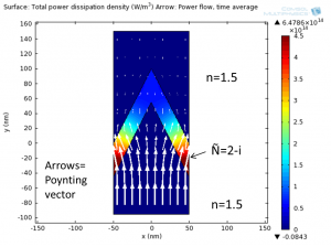
- Figure 1: Model of power flow and absorption of single nanowedge unit cell. Arrows designate the Poynting vector of time-averaged power flow. Absorbing active layer is sandwiched between layers of glass. Incident light is TE polarized and varied from 300 to 900 nm.
-
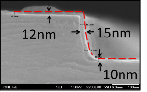
- Figure 2. All-dry deposited PEDOT is shown to conformally coat a nanoscale feature. This uniform thickness over sharp features is a substantial improvement over the non-conformal coating properties of spun-coat PEDOT:PSS on features of the same scale.
- P. Peumans, A. Yakimov, and S. R. Forrest, “Small molecular weight organic thin-film photodetectors and solar cells,” Journal of Applied Physics, vol. 93, p. 3693, Apr. 2003. [↩]
- V. Karagodsky, F. Sedgwick, and C. J. Chang-Hasnain, “New Physics of Subwavelength High Contrast Gratings,” Quantum Electronics and Laser Science Conference OSA Technical Digest Optical Society of America, 2011. [↩]
- S. Mallick, N. P. Sergeant, M. Agrawal, J. Lee, and P. Peumans, “Coherent light trapping in thin-film photovoltaics,” Materials Research Society Bulletin, vol. 36, no. 06, pp. 453 – 460, 2011. [↩]
- K. Nalwa, J. M. Park, K. M. Ho, and S. Chaudhary, “On realizing higher efficiency polymer solar cells using a textured substrate platform,” Advanced Materials, vol. 23, pp. 112-116, 2011. [↩]
- A. Raman, Z. Yu, and S. Fan, “Dielectric nanostructures for broadband light trapping in organic solar cells,” Optics Express, vol. 19, pp. 19015-19026, 2011. [↩]
- S. B. Rim, S. Zhao, S. R. Scully, M. D. McGehe, and P. Peumans, “An effective light trapping configuration for thin-film solar cells,” Applied Physics Letters, vol. 91, p. 243501, 2007. [↩]
- S. GACS Nano. vol. 2(9), pp. 1959-67, 2008. [↩]