Heat Transport in Nanostructured Materials
- Category: Energy, Materials, Nanotechnology
- Tags: jolene mork, william tisdale
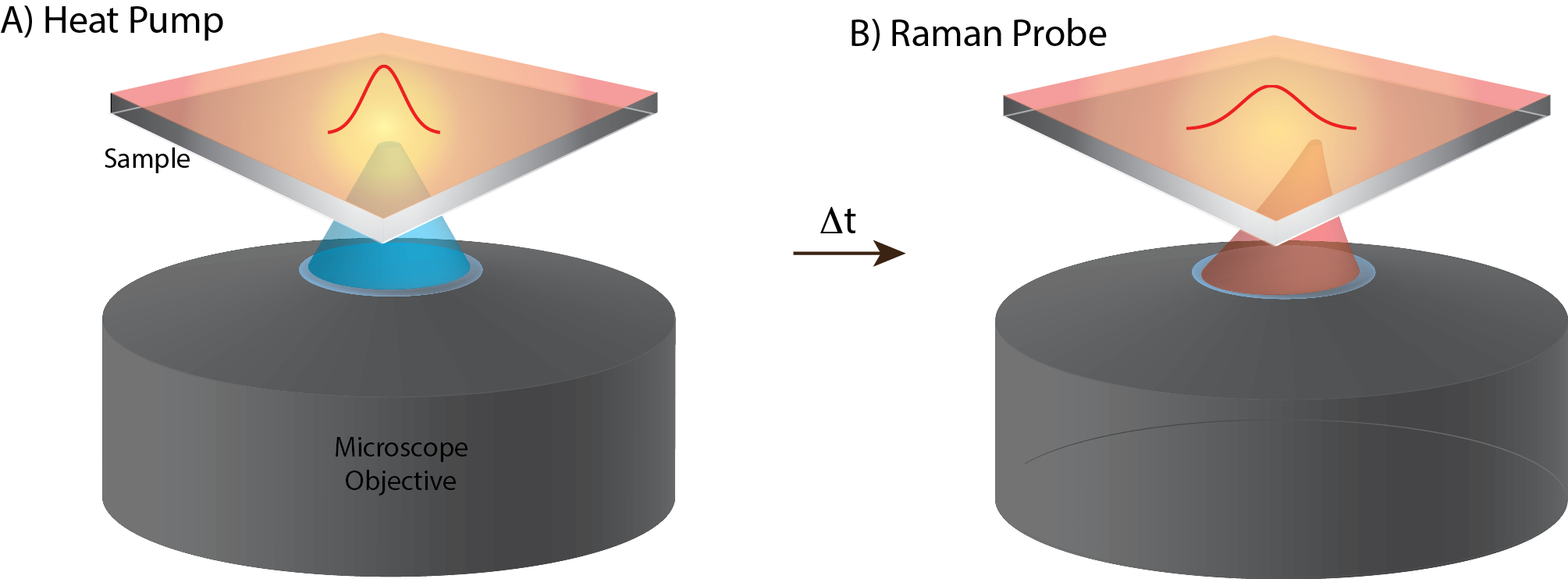
Figure 1: Time-resolved anti-Stokes Raman imaging schematic. A) A high-energy pulsed laser excites and locally heats the sample with a Gaussian excitation profile. B) After a variable delay time Δt, the Raman probe laser measures the anti-Stokes scattered signal at a known distance from the excitation source. By varying the position and time between the laser pulses, we will map the thermal properties of our samples.
Thermal management in nanoscale materials dramatically affects the efficiency of novel energy generation technologies, and engineering devices with appropriate heat transport properties is requisite for their success. We are using Raman spectroscopy to measure and visualize heat transport in nanostructured materials, such as organic/polymeric or quantum dot thin films, which may be used for photovoltaic or thermoelectric devices. Raman spectroscopy measures the inelastic scatting of light off a sample, and the resulting spectrum contains a chemical fingerprint of the molecules involved in heat transport as well as a measure of local temperature via vibrational excitations. In particular, through pulsed local heating of a sample and measuring the temperature of a nearby point a known distance and time away with Raman spectroscopy, we can visualize thermal diffusion and unveil the vibrational pathways involved[1][2].
Our unique setup allows for spatial, temporal, and spectral resolution of our Raman signal, which allows us to extract data related to the mechanism and efficiency of heat diffusion on the length scales over which it occurs. We have built a Time-resolved anti-Stokes Raman imaging microscope (see Figure 1), allowing us to collect point-by-point vibrational occupation information through laser scanning of our Raman probe beam relative to a heat pump. With this setup, we will be able to change the composition or architecture of our samples in known ways and measure the resulting changes in heat transport efficiency. In this way, our studies will inform engineering of higher quality devices by improving thermal management within the nanostructured films.
- T. Beechem, J. Serrano. “Raman Thermometry of Microdevices: Choosing a Method to Minimize Error,” Spectroscopy, vol. 26, no. 11, pp 36-44, November 2011. [↩]
- T. Beechem, S. Graham. “Temperature Measurement of Microdevices using Thermoreflectance and Raman Thermometry,” in BioNanoFluidic MEMS edited by P.J. Hesketh. Springer, 2008. [↩]