category » Electronic Devices
Due to its high band gap energy and superb electronic-carrier mobilities, GaN is fast becoming the material of choice for…

Gallium nitride (GaN)-based electronics are one of the most exciting areas of innovation for high-frequency and high-voltage semiconductor devices. Although…
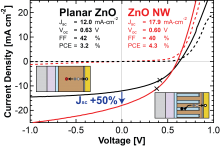
Semiconducting nanowire-based solar cells have gained interest because of their potential to achieve one-dimensional charge transport pathways and large interfacial…
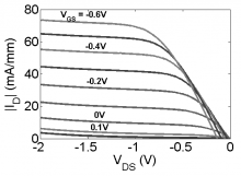
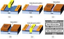
Ge nanowires are of interest for future sub-10-nm gate length p-MOSFETs because of the excellent electrostatic control afforded by the…
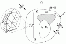
Domain decomposition concepts, combined with other high performance scientific computation technologies, provide a framework to hybridize different solvers together and…
The use of magnetic forces to improve fluidic self-assembly of micro-components has been investigated using Maxwell 3D to model the…
For decades, growth and innovation in the microelectronics industry has been fueled by the aggressive scaling of silicon complementary metal…
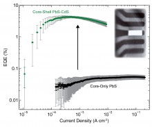
Here we demonstrate a solution-processed ordered bulk heterojunction quantum dot (QD) solar cell with AM1.5G power conversion efficiencies of up…
Engineering energy-efficient power electronic systems has recently attracted tremendous interest. Similarly, the gallium nitride metal-insulator-semiconductor high-electron-mobility transistor (GaN MIS-HEMT) fabricated…
With its rich physics, graphene has properties that make it a viable candidate for implementing electronic devices. For example, graphene…
State-of-the-art ultrafast cathodes are based on the photoelectric effect, where electrons are emitted from a flat surface using ultraviolet (UV)…
Field emission arrays (FEAs) are an attractive alternative to mainstream thermionic cathodes, which are power hungry and require high vacuum…
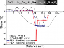
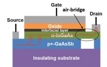
In the last few years, III-V compound semiconductors have emerged as a promising family of materials to replace silicon in…
As silicon metal-oxide-semiconductor field-effect transistors (MOSFETs) keep scaling down in size, fundamental physical limits threaten the continued improvement on their…
Colloidal semiconductor nanocrystals or quantum dots (QDs) offer size-tunable absorption and luminescence spectra, permitting a broad range of applications in…
Nanostructured photocathode arrays can be used as the electron sources for the compact coherent X-ray source. Femtosecond laser pulses were…
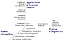
Due to the growing populations in cities, resources for city and village residents have become scare while costs for public…
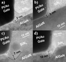
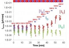
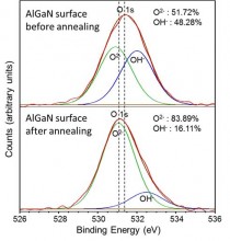
AlGaN/GaN High Electron Mobility Transistors (HEMT) are candidate for high-power amplifiers. However, for wide scale implementation reliability issues for these…
Near-infrared light sources integrated at room temperature with any planar surface could be realized by harnessing the broad spectral tunability,…
GaN FETs offer superior advantages in high-voltage and high-temperature operation due to its large bandgap (3.4 eV) and high breakdown…
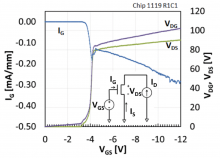
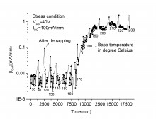
GaN-based high-electron-mobility transistors (HEMTs) are very promising candidates for the next generation of high-power and high-frequency electronics. However, trapping effects…
Nanostructured solar cells attract increasing attention as a promising photovoltaic (PV) technology[1]. Generation of free charge carriers in nanostructured PV…
With the silicon-based electronics reaching physical limits that inhibit continued improvements in device performance, much research has been directed towards…
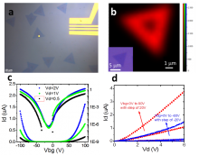
Tunneling field-effect transistors (TFETs)[1] are promising for low-power applications due to their potential to achieve a subthreshold swing (SS) lower…
After enabling much of the modern world for more than 60 years, in the near future electronics will develop in…
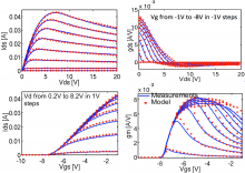
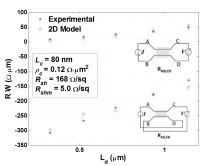
Compact models of GaN-based high-electron-mobility transistors (HEMTs) are essential for the design of power conversion circuits such as power integrated…
Si-based CMOS technology is approaching the limits of its capabilities, and as a result there is extensive research into looking…
Wide band-gap III-nitride semiconductors have excellent potential for next-generation power electronics systems. AlGaN/GaN high-electron-mobility transistors (HEMTs) have attracted great interest…
In this research we seek to develop acousto-optic, guided-wave modulators in proton-exchanged lithium niobate[1] for use in holographic and other…
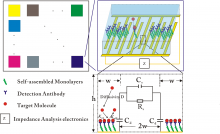
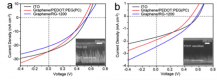
Immunoassays use antibodies to detect protein biomarkers, with a substantial global market and significant importance for clinical practice. However, traditional…
With the continuing downscaling of the modern complementary metal–oxide–semiconductor (CMOS) technology, integrated circuit power consumption has become one of the…
Achieving a sharp subthreshold swing (S) is crucial to enable the supply voltage scaling that is necessary to reducing power…
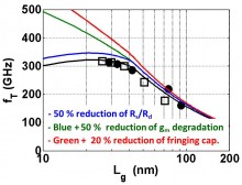
The high-frequency performance of GaN-based high-electron-mobility transistors (HEMTs) has been significantly improved over the last two decades. State-of-the-art devices have…
The performance of GaN-based high-electron-mobility transistors (HEMTs) has been significantly improved over the last two decades through extensive research[1][2][3]. However,…
Currently bulk Bi and BixSb1-x have the best known thermoelectric (TE) properties at cryogenic temperatures. These properties can be further…
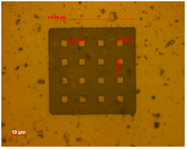
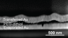
Transfer printing of thin metal films enables the fabrication of both planar and suspended membrane electrodes for microelectromechanical (MEMS) sensors…
Quantum dots (QDs) are exciting materials because their bandgap is dependent on the dot size. The use of QDs allows…
Due to the wide band gap energy and high breakdown electric field of GaN, heterostructure transistors made from it are…
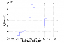
Detection of high-energy radiation (e.g., γ-rays) is key in nuclear non-proliferation strategies. When a wide-band gap semiconductor detector intercepts a…