Recombination Dynamics of Charge Carriers in Nanostructured Solar Cells
- Category: Electronic Devices, Energy, Materials, Nanotechnology
- Tags: andrea maurano, vladimir bulovic
Nanostructured solar cells attract increasing attention as a promising photovoltaic (PV) technology[1]. Generation of free charge carriers in nanostructured PV devices occurs at the electron donor-acceptor interface, analogous to a pn-junction interface in traditional crystalline Si solar cells. Recombination at this interface constitutes a major pathway of charge carrier loss. Characterizing and controlling recombination dynamics are key to informing design of novel device architectures. Recombination parameters also enable comparisons between different device architectures.
This work uses the transient optoelectroic techniques[2] to probe recombination mechanisms under standard operating conditions in four solar cells. Figure 1 shows the cells: a lead sulfide quantum dot and zinc oxide (QD PbS:ZnO) pn-heterojunction, a chloroaluminium phthalocyanine and fullerene (ClAlPc:C60) planar heterojunction, a tetraphenyldibenzoperiflanthene and C60 (DBP:C60) planar heterojunction, and a DBP and C60 planar mixed heterojunction (DBP:( DBP/C60):C60). Figure 2a shows charge carrier lifetimes as functions of the open-circuit voltage. Varied carrier lifetimes may arise from interface morphologies: e.g.,, the slower recombination transients observed in the DBP:C60 devices may be due to their intrinsic planarity. We measure charge carrier density as a function of the open circuit voltage, as in Figure 2b. Combining carrier lifetime and charge carrier density allows us to calculate recombination rates and assign the major recombination to a dominant mechanism. In all devices, the relevant recombination is a geminate recombination of excitons or standard SRH recombination (PbS:ZnO solar cells) and a non-geminate recombination between two free charges. Investigating the type of recombination is critical for designing solar cells with improved efficiency.
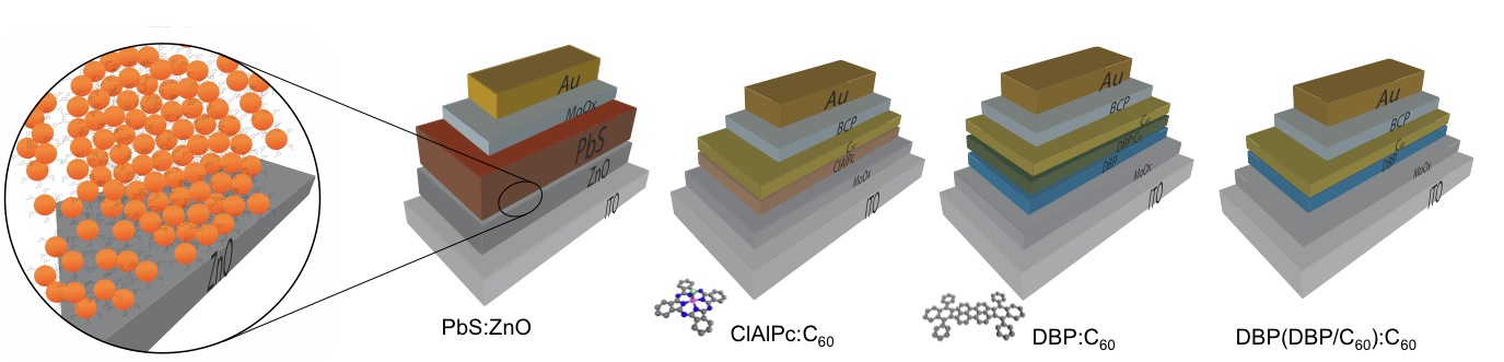
Figure 1: Schematics of nanostructured PV architectures studied in this work. Left to right: QD PbS:ZnO pn-heterojunction (inset shows cartoon of QD passivated by organic ligand on ZnO), ClAlPc:C60 planar heterojunction with ClAlPc molecular structure, DBP:C60 planar heterojunction with DBP molecular structure, and DBP:( DBP/C60):C60 planar mixed heterojunction. All devices are sandwiched between an electron and hole transporting layer such as bathocuproine and molybdenum oxide and ITO and Au as electrodes.
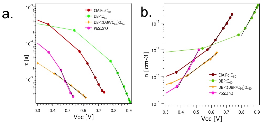
Figure 2: a) Charge carrier lifetime and b) charge carrier density as function of open circuit voltage for ClAlPc:C60, DBP:C60, (DBP:( DBP/C60):C60), and PbS:ZnO.
- Anonymous, “A sunny outlook,” Nature Photonics, vol. 6, no. 3, p. 129, Mar. 2012. [↩]
- C. G. Shuttle, B. O’Regan, A. M. Ballantyne, J. Nelson, D. D. C. Bradley, J. de Mello, and J. R. Durrant, “Experimental determination of the rate law for charge carrier decay in a polythiophene: Fullerene solar cell,” Applied Physics Letters, vol. 92, p. 3, 2008. [↩]