Enhancement of Antimonide-based P-channel FETs using Process-induced Strain
- Category: Electronic Devices
- Tags: jesus del alamo, luke guo
For decades, growth and innovation in the microelectronics industry has been fueled by the aggressive scaling of silicon complementary metal oxide semiconductor (CMOS) technology. However, as silicon devices scale to the nanometer regime and their intrinsic limitations become more pronounced, the role of silicon in state-of-the-art logic devices is being called into question. Consequently, III-V semiconductors have gathered great interest as a channel material to replace silicon, largely due to their impressive electron transport properties and the successful demonstration of outstanding n-channel devices[1]. On the other hand, this success has not yet been translated to III-V p-channel devices because of the low intrinsic hole mobilities of most III-V semiconductors. Developing a high performance p-channel device is critical to the realization of a future III-V CMOS architecture to extend the semiconductor roadmap and enable future novel semiconductor technologies.
A promising solution to the III-V p-channel problem is the use of antimonides, which have the largest hole mobilities of any III-V material system. The performance of antimonide devices can be further enhanced by strain, which has already found great success in high-volume silicon manufacturing. Chip-bending experiments using antimonide p-channel FETs have shown that antimonides respond favorably to strain[2]. In this work, we show that the performance of p-channel antimonide FETs can be further enhanced using a compressively stressed nitride layer[3].
Compressively stressed p-channel FETs with a 0.5-μm gate length were fabricated using a 7.5-nm In0.41Ga0.59Sb channel. Figures 1 and 2 show, respectively, the output characteristics and transconductance gm of a typical transistor. A peak gm of 115 mS/mm was obtained, comparable to similarly fabricated unstressed devices with a gate length of 0.25 μm, despite having a gate length twice as long. This peak gives strong evidence for stress-induced transport enhancement.
Ongoing work includes efforts to fabricate shorter-channel transistors to capture even more stress enhancement, as simulations project the gains from stress to increase with gate length scaling.
-
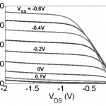
- Figure 1: Output characteristics of In0.41Ga0.59Sb pFET with Lg = 0.5 μm fabricated with a stressed nitride layer. The device shows good saturation characteristics. The large gate leakage is under investigation.
-
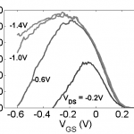
- Figure 2: Transconductance of Lg = 0.5 μm device with a stressed nitride layer. A peak transconductance, gm, of 115 mS/mm was obtained.
- J. A. del Alamo, “Nanometer-scale electronics with III-V compound semiconductors,” Nature, vol. 479, no.7373, pp. 317-323, Nov. 2011. [↩]
- L. Xia, J. B. Boos, B. R. Bennett, M. G. Ancona, and J. A. del Alamo, “Hole mobility enhancement in In0.41Ga0.59Sb quantum-well field effect transistors,” Applied Physics Letters, vol. 98, no 5, 053505, Feb. 2011. [↩]
- L. Xia, V. Tokranov, S. R. Oktyabrsky, and J. A. del Alamo, “Performance enhancement of p-channel InGaAs quantum-well FETs by superposition of process-induced uniaxial strain and epitaxially-grown biaxial strain,” in IEDM ’11 Technical Digest, pp. 315-318, Dec. 2011. [↩]